


















Lesson 45 of 45 · Projects and Practice
Further study: where to go after PCB design
Plan your next steps after PCB design: circuit analysis, analog and power electronics, embedded systems, RF, standards and tools, with a study path and project ideas.
You can now take a board from idea to files, predict some of its problems before they happen, and bring it up methodically. That is a real skill set, and it opens several directions. This lesson maps the neighboring subjects, suggests a study path for each goal, and lists the standards and tools that professionals use.
What you will learn
- Choose a next subject based on what you want to build.
- Know the standards and tools worth learning.
- Plan a sequence of projects that deepens your skills.
Key terms
IPC standards: industry documents (IPC-2221 design, IPC-7351 land patterns, IPC-A-610 acceptability of assemblies, J-STD-001 soldering).
Simulation: predicting circuit behavior with software before building.
Revision: a numbered version of a board (rev A, rev B).
Certification: formal testing for emissions and safety (for example CE, FCC, UL).
Choose by goal
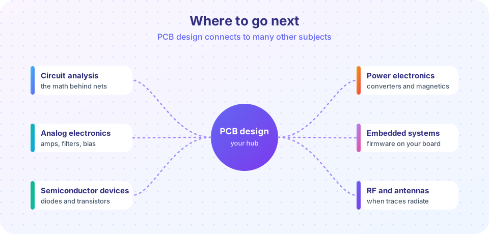
| If you want to... | Study next |
|---|---|
| Understand the math behind every net | Circuit analysis |
| Design amplifiers, filters and sensor front-ends | Analog electronics |
| Understand how diodes and transistors really behave | Semiconductor devices |
| Build converters, chargers and motor drives | Power electronics |
| Write firmware for your boards | Embedded systems |
| Work with radios, antennas and fast links | RF and antennas |
These tracks complement this one: PCB design tells you how to put circuits on a board, and each subject tells you which circuit to put there. Return to the PCB design track page when you want a refresher.
A study path
- Build the three mini projects and write a design review for each.
- Pick one direction from the table and complete its first chapters.
- Design a revision B of an earlier board that fixes what you learned: a smaller loop, better test points, a cleaner stackup.
- Learn your tools deeply. A free, open-source CAD suite is enough to design professional boards: learn its rule editor, scripting or plugins, and the 3D viewer.
- Read datasheets and reference designs critically. Layout guidelines in power-IC, USB and RF datasheets are free lessons from the people who designed the chips.
- Learn to simulate. SPICE for circuits, field solvers for impedance, and thermal estimators for copper and heat.
- Study standards when you ship products: IPC, safety and EMC rules vary by market.
Where PCB design leads
- Hardware startups and consumer products: prototype fast, test early, design for manufacture.
- Industrial and automotive: reliability, creepage and clearance distances, conformal coating, long lifetimes.
- High-speed digital: DDR, PCIe and multi-gigabit links need field solvers, length matching and careful stackups.
- RF: controlled impedance, shielding, antenna layout.
- Power: thermal design, high-current copper, magnetics, safety isolation.
Common misconceptions
"I need an expensive tool." Free, professional-quality PCB tools exist; skill matters more than price.
"One perfect board comes out of the first design." Professionals plan for revisions and budget time for them.
"Layout is separate from circuit design." In fast and power circuits, layout is part of the circuit.
Try it
Press Run (or Ctrl + Enter) to see the console output here.
No output.
Check your understanding
Quick check · 3 questions
of 3 answered You scored / 3 · perfect!
-
1. Which IPC document defines standard land patterns?
IPC-7351 covers land pattern design. -
2. Which next subject fits designing a battery charger?
Chargers are converters. -
3. What is a good habit when a board has problems?
A revision log turns mistakes into improvements.
Summary
- PCB design connects to circuits, power, embedded and RF subjects.
- Choose a next subject by what you want to build, and keep building boards.
- Learn the standards and tools as your projects demand them.
- Treat every revision as a lesson.
Return to the PCB design track page.
Track your progress
Create a free account to tick off lessons and pick up where you left off on any device.
of PCB Design and Prototyping lessons completed