


















Lesson 18 of 45 · Layout and Routing
Placement Strategy
Learn how to place parts on a PCB: group by function, put connectors at the edge, decoupling capacitors at the pins and crystals close to the chip, and measure wire length.
If you only learn one skill in layout, make it placement. Parts that are well placed are connected by short, straight traces. Parts that are badly placed are connected by long, winding ones that cross each other, need more layers and pick up noise. A good placement can often be routed in an hour; a bad one can occupy a week and still never work properly.
Placement is also the most creative part of layout. There is no single right answer, but there are many wrong ones, and there are reliable principles that keep you out of trouble.
What you will learn
- How to place parts in functional zones
- Where connectors, regulators, decoupling capacitors and crystals go
- How to estimate wire length from a placement
- Why trace inductance makes decoupling distance matter
Key terms
Ratsnest (airwires): straight lines that show the connections still to be routed.
Decoupling (bypass) capacitor: a small capacitor next to a power pin that supplies fast current pulses locally.
Floorplan: the rough allocation of board regions to functions.
HPWL: half-perimeter wirelength, a quick estimate of the length of a net.
Thermal zone: an area where hot parts are kept apart from heat-sensitive ones.
Start with the floorplan
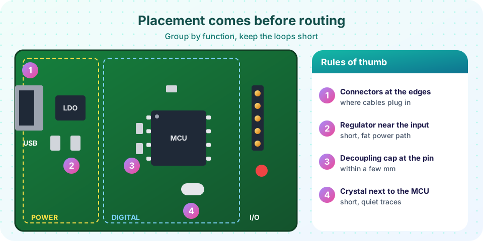
Before placing individual parts, divide the board into zones. A typical mixed board has:
- a power zone where the input connector and regulators sit, close to where the power enters;
- a digital zone with the microcontroller or logic;
- an analog or sensor zone, kept away from switching noise;
- an I/O zone along an edge, with connectors for the outside world.
Signals should travel across the board in a clean direction, for example power from left to right and I/O at the far side. When two zones need to talk, they should do it across a short, well-defined boundary. This is a rough guide, not a law; small boards may have no real zones.
Placing the parts
Fixed parts first. Connectors, buttons, LEDs, displays and mounting holes are placed according to the case. Put connectors on edges, because cables enter from outside and need to be reachable. Heavy parts should be near mounting holes and not overhang a flexible edge.
Key IC next. Put the main chip near the centre of its zone, oriented so that the pins that connect to the busiest neighbours face them.
Decoupling capacitors at the power pins. Every IC has a small capacitor (typically 100 nF) between each supply pin and ground. Its job is to supply the burst of current the chip draws each time it switches, so that the burst does not have to come all the way from the regulator. For this to work, the capacitor's loop (capacitor, via or trace to power pin, chip, ground return) must be short. A rule of thumb for trace inductance is about 1 nH per millimetre (10 nH/cm). At 100 MHz one nanohenry has a reactance of 2π × 100e6 × 1e-9 = 0.63 Ω, so a 10 mm detour adds more than 6 Ω in series with the capacitor and ruins its effect. Put the capacitor within a few millimetres, with the capacitor's pad between the supply pin and the via to the plane.
Crystals and oscillators sit right next to the chip's clock pins, with short, equal traces and a ground area beneath or around them. Keep noisy traces away.
Regulators go near the input connector; their input and output capacitors sit right at their pins. For switching regulators, the loop of input capacitor, switch and inductor is the most critical layout in the whole board: follow the datasheet's example layout exactly.
Heat producers (power transistors, regulators, LEDs) are spread out and given copper area. Keep sensitive parts like sensors, crystals and electrolytic capacitors away from them.
Orientation and grid. Align passives in rows with the same orientation; assembly is easier, inspection faster and the board looks professional. Use a grid, such as 0.5 mm or 1 mm, so that parts and traces stay tidy.
Measuring a placement
A cheap quality number is the total estimated wire length. For each net, take the smallest rectangle that encloses all its pads; its half-perimeter (width plus height) is the HPWL. Summing over nets gives a quick estimate of how much copper the placement needs. Software placers use this idea, and you can use it to compare two arrangements. In the first example below, you will compute it.
A note on accessibility
Leave room for the soldering iron and for probes. Keep tall parts from shadowing small ones during reflow and during inspection. Put test points on key nets such as power rails and communication lines, with 1.5 mm or larger pads, on the side you can reach. You will thank yourself in Chapter 7.
Common misconceptions
"The autorouter will sort out a messy placement." Autorouters follow your placement. Messy input gives messy output.
"Decoupling capacitors can be anywhere near the chip." Distance matters: millimetres of trace add nanohenries, and nanohenries limit how fast the capacitor can respond.
"Placement is finished once everything fits." A placement that fits is only the start. Check wire length, loops, heat and access for soldering and testing.
Try it
The first example estimates the half-perimeter wirelength of two placements of the same four parts. Positions are in millimetres. Try moving the parts to find a placement that beats both.
Press Run (or Ctrl + Enter) to see the result here.
Program input · what you'd type while the program runs
Type the answers before you press Run, one per line. Each time the program reads a line (with input()), it gets the next line from this box.
The second example is an interactive decoupling-distance demo. Slide the capacitor away from the chip and watch the series inductance and its reactance at 100 MHz grow. The 1 nH per millimetre figure is a rule of thumb.
Check your understanding
Quick check · 5 questions
of 5 answered You scored / 5 · perfect!
-
1. Where should a decoupling capacitor be placed?
A short loop keeps inductance low so the capacitor can respond quickly. -
2. Roughly how much inductance does 1 cm of trace have?
The rule of thumb is about 1 nH per mm, or 10 nH per cm. -
3. Where do connectors normally go?
Cables and plugs come from outside the board. -
4. What does HPWL estimate?
Half-perimeter wirelength is the bounding-box width plus height. -
5. Why leave test points on key nets?
Test points let you measure signals during bring-up.
Summary
- Divide the board into zones, place fixed parts first, then the key IC.
- Put decoupling capacitors at the power pins; trace inductance is about 1 nH per millimetre.
- Group parts, align passives and leave room for soldering and probing.
- Compare placements by estimated wire length before routing.
Next: Trace Width and Current
Track your progress
Create a free account to tick off lessons and pick up where you left off on any device.
of PCB Design and Prototyping lessons completed