


















Lesson 3 of 45 · Getting Started
Layers, Copper Weight and Materials
Understand PCB layer counts, copper weight in ounces, core and prepreg, and why a four-layer stack-up with ground and power planes is so popular.
The simplest PCB has copper on one side only. The boards inside a modern smartphone have ten or more layers, pressed together like a lasagna and thinner than a coin. Why would anyone pay for more layers? Because each layer is more room to route traces, and some layers can be dedicated to jobs that make a board electrically quieter: a solid ground plane and a solid power plane.
In this lesson you learn how the layers are built, what "1 oz copper" means, how to read a stack-up, and how to choose between two and four layers for a first design.
What you will learn
- The difference between core and prepreg, and how a board is laminated
- What copper weight in ounces means in micrometres
- How to read a four-layer stack-up
- When two layers are enough and when to use four
Key terms
Layer: one sheet of copper in the stack. Counted as 1, 2, 4, 6 and so on.
Core: a rigid sheet of cured FR-4 with copper already bonded to both sides.
Prepreg: "pre-impregnated" fiberglass, a half-cured glue layer that bonds cores together under heat and pressure.
Copper weight: the thickness of copper, given as ounces per square foot (1 oz = about 35 µm).
Stack-up: the ordered list of copper, core and prepreg layers with their thicknesses.
Plane: a layer (or most of it) filled with solid copper, normally ground or power.
How a multilayer board is made
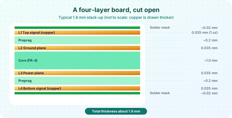
A two-layer board is a single core with copper on both sides. A four-layer board is built from a core with copper on both faces (which become layers 2 and 3), a sheet of prepreg on each side and a copper foil on the outside. The stack is pressed in a hot press; the prepreg melts, flows and cures, gluing everything together. Then holes are drilled and plated, the outer layers are etched and the solder mask is added.
The result is symmetric: the same thickness above and below the core. This matters because unequal copper or dielectric makes a board bow or twist when it is heated in the soldering oven.
Typical numbers for a 1.6 mm four-layer board are 0.035 mm for each copper foil (1 oz), about 0.2 mm of prepreg on each side, and about 1.0 mm for the core. Fabs publish their own stack-ups, and you should use theirs in your CAD tool rather than guess.
Copper weight
Copper thickness is specified in a curious unit: ounces per square foot. One ounce of copper spread evenly over one square foot is about 35 µm (more precisely 34.8 µm) thick. So:
| Weight | Thickness | Typical use |
|---|---|---|
| 0.5 oz | about 17 µm | inner layers on dense boards, fine-pitch traces |
| 1 oz | about 35 µm | default for most boards |
| 2 oz | about 70 µm | power boards with high current |
Thicker copper carries more current for the same width but is harder to etch finely, so minimum trace width and spacing grow with weight. Most low-cost fabs build 1 oz outer layers and 0.5 oz inner layers by default.
Sheet resistance is a handy figure. For a square piece of copper, the resistance between opposite edges is ρ / t whatever the size of the square. For 1 oz copper this is 1.68e-8 / 35e-6, which is about 0.48 mΩ per square. A trace that is ten squares long (length ten times its width) has about 4.8 mΩ. That makes a quick mental estimate easy: count the squares.
Why four layers?
A four-layer board usually uses the order signal, ground, power, signal. This brings three benefits.
- Ground plane. Every signal on the top layer has a solid reference just 0.2 mm away. The return current flows right underneath the trace, so loops are small and noise is low. Chapter 4 and 5 explain the physics.
- Easy power. A power plane delivers a voltage everywhere on the board. A short via connects any pin to it, so you avoid long power traces.
- More routing room. Signals can use both outer layers without crossing the planes.
A two-layer board costs less (often half as much), and for slow circuits with few parts it is perfectly fine: one layer for signals, one mostly ground. As a rule, move to four layers when you have fast signals, a microcontroller with many pins, dense packages or noise-sensitive analog parts.
Materials beyond FR-4
FR-4 is a family; many grades exist. The main numbers are the glass transition temperature (Tg, where the resin softens; common values are 130 to 170 °C) and the dielectric constant (εr, about 4.2 to 4.6 at low frequency for FR-4). The dielectric constant changes the speed of signals and the impedance of traces, which you will use in Chapter 5.
Other materials serve special jobs. Aluminium-core boards spread heat from LEDs. Polyimide makes flexible boards that bend. PTFE-based laminates (such as Rogers materials) have low loss at radio frequencies, and they cost many times more than FR-4. For learning and most products you will use FR-4.
Common misconceptions
"More layers is always better." More layers cost more and the layout can still be bad. A well-laid two-layer board beats a careless four-layer one.
"1 oz copper is 1 ounce of weight on my board." It is a thickness convention (the copper foil that would weigh 1 oz per square foot), not the weight of your board.
"The stack-up is the fab's problem." The stack-up determines trace impedance and plane spacing, so you must choose it and check it with the fab before routing.
Try it
The first example is a stack-up calculator in Python. Edit the layer list, and the code prints the total thickness and draws the stack. A real 1.6 mm board is rarely exactly 1.60 mm; the tolerance is typically about ±10 %.
Press Run (or Ctrl + Enter) to see the result here.
Program input · what you'd type while the program runs
Type the answers before you press Run, one per line. Each time the program reads a line (with input()), it gets the next line from this box.
The second example is an interactive copper-weight explorer. Slide the weight and watch the thickness and the sheet resistance change. Resistance per square halves when the copper doubles.
Check your understanding
Quick check · 5 questions
of 5 answered You scored / 5 · perfect!
-
1. About how thick is 1 oz copper?
1 oz per square foot is about 34.8 µm, usually rounded to 35 µm. -
2. What does prepreg do?
Prepreg melts and cures under the press, gluing cores and foils into one board. -
3. The usual layer order of a simple four-layer board is
Outer layers route signals; the inner planes give ground and power. -
4. What is the resistance per square of 1 oz copper (approximately)?
ρ/t = 1.68e-8 / 35e-6 ≈ 0.48 mΩ per square. -
5. When is a two-layer board usually enough?
Slow, simple circuits work well on two layers; fast or dense ones benefit from planes.
Summary
- Multilayer boards are laminated from cores and prepreg with copper foils on the outside.
- 1 oz copper is about 35 µm; sheet resistance is about 0.48 mΩ per square.
- Four layers (signal, ground, power, signal) give a solid return path and easy power.
- FR-4 is the default; special materials serve heat, flexing and radio frequencies.
Track your progress
Create a free account to tick off lessons and pick up where you left off on any device.
of PCB Design and Prototyping lessons completed