


















Lesson 21 of 45 · Layout and Routing
Ground Planes and Return Paths
Understand why every signal needs a return path, how return current follows the trace over a ground plane, and why slots, splits and long detours cause noise and EMI.
Current always flows in a loop. When a signal leaves a chip through a trace, an equal current must come back to the chip, otherwise charge would pile up somewhere. The wire you draw is only half of the circuit; the other half is the return path, and you rarely draw it. On a PCB it is usually the ground, and on a good board it is a solid plane right under the trace.
This is the single most useful idea in PCB layout, and it explains an enormous list of design rules: why ground planes exist, why you should not cut them, why decoupling capacitors sit close to pins, and why a noisy board often turns out to have a hidden big loop.
What you will learn
- Why every signal is a loop and what loop area means
- How return current chooses its path at low and high frequency
- Why a ground plane helps, and how to avoid slots and splits
- How to use ground pours and stitching vias on two-layer boards
Key terms
Return path: the route that current takes back to its source.
Loop area: the area enclosed by the signal path and its return path; bigger loops radiate and pick up more noise.
Ground plane: a layer (or most of it) of solid copper connected to ground.
Slot (split): a gap in a plane, for example between two copper pours or around a via row.
Stitching vias: vias that tie ground areas on different layers together.
Why the loop matters
Imagine a loop of wire. A changing current in it creates a magnetic field, and a changing field through it induces a voltage. The two effects are proportional to the area of the loop. A large loop is both a better antenna (it radiates, causing EMI problems) and a better receiver (it picks up noise). It also has more inductance, which slows fast edges and makes voltage spikes.
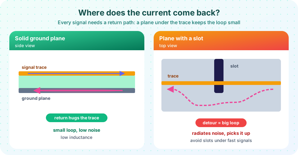
So the goal in layout is to keep the loops small: a small loop radiates little, picks up little and has low inductance. A signal trace over a plane has a loop area equal to its length times the height h of the dielectric between trace and plane. With h = 0.2 mm that is tiny. Without a plane, the return might be a long ground trace a centimetre away: a loop 50 times larger.
How the return current chooses
Current takes the path of least impedance. At DC and very low frequencies, the impedance is just resistance, so current spreads through all available copper. As frequency rises, inductance dominates, and the lowest-impedance path is the one with the smallest loop, which means the return current runs in the plane directly under the trace, mirroring it.
Over a plane, the return current density has a bell shape centred under the trace. A standard result for a thin trace at height h over a plane is that the fraction of the return current within a distance x of the trace centre is (2/π) × arctan(x/h). So half the current is within h of the trace, 80 % within about 3 h and 94 % within 10 h. With a thin dielectric, almost all the return current sits directly under the signal. This is why a plane close to the signal layer is so effective, and why the four-layer stack-up puts the ground plane right beside the top signal layer.
The "frequency at which this starts" is about 1 MHz or lower for typical traces. Practically, every digital signal with edges faster than a few nanoseconds has content far above that, so it follows the plane.
What goes wrong: slots, splits and gaps
If the plane under the trace has a gap, the return current cannot go straight. It must detour around the gap, and the loop it makes grows from trace length × h to a loop that is millimetres or centimetres wide. The result: radiated noise (EMI), crosstalk into nearby traces and ringing. Common ways to create slots:
- A row of vias or a long thin connector footprint cutting across the plane, because their clearance rings merge.
- Splitting ground into "analog" and "digital" areas and then routing signals across the split.
- Routing a trace on the plane layer, cutting the plane (a trace on the ground layer is a slot).
- Large keep-out regions under connectors or antennas.
Remedies: avoid routing under a gap; if a gap is unavoidable, route the signal around it. When a signal changes reference plane through a via, put a stitching via right next to it. Prefer one solid ground plane for the whole board and keep analog and digital circuits separate by placement, not by cutting the plane.
Two-layer boards: ground pours
Without a dedicated plane, you can still follow the same principle. Route signals on the top and use the bottom as mostly ground: a copper pour (zone) connected to ground. Place ground vias around the board and next to signal vias. Route the critical return in a straight, short path. Where a signal runs for a long distance, keep its ground return beside or below it. A two-layer board with a good bottom ground pour behaves much better than one with scattered ground traces, but a plane at 0.2 mm is still far closer than a bottom pour at 1.6 mm. This is another reason fast designs use four layers.
Common misconceptions
"Ground is a single point with zero voltage." Ground is a conductor with resistance and inductance. Current through it creates small voltages, and the loop it forms matters.
"Splitting the ground plane keeps noise out of analog circuits." It often does the opposite by forcing return currents around the split. Use placement and a solid plane.
"Only high-speed boards need to worry." Even slow boards with switching regulators and motors can have noisy loops that upset sensors.
Try it
The first example plots how the return current is distributed under a trace for several dielectric heights. The lower the dielectric, the tighter the current hugs the trace.
Press Run (or Ctrl + Enter) to see the result here.
Program input · what you'd type while the program runs
Type the answers before you press Run, one per line. Each time the program reads a line (with input()), it gets the next line from this box.
The second example draws the loop. Choose the height of the plane below the trace, and the length of a detour caused by a slot; the page shows the loop area and compares it with an ideal solid plane. The model is geometric (area of a rectangle), not a field simulation.
Check your understanding
Quick check · 5 questions
of 5 answered You scored / 5 · perfect!
-
1. Why do loops matter on a PCB?
Loop area controls radiation, noise pickup and inductance. -
2. At high frequency, where does the return current flow?
It takes the path with the smallest loop inductance, which is under the trace. -
3. What does a slot in the ground plane under a signal do?
The return cannot cross the gap, so it goes around. -
4. A signal changes layers through a via between two ground planes. What helps?
The return current needs a short way to change planes. -
5. How can a two-layer board mimic a plane?
A solid ground pour gives a return path, though farther away than a 4-layer plane.
Summary
- Every signal is a loop; loop area drives radiation, pickup and inductance.
- High-frequency return current flows in the plane right under the trace.
- Never route over slots or splits; stitch layer changes with ground vias.
- On two-layer boards use a ground pour and short, direct returns.
Next: Chapter 4 Review
Track your progress
Create a free account to tick off lessons and pick up where you left off on any device.
of PCB Design and Prototyping lessons completed