


















Lesson 25 of 45 · Signal and Power Integrity
Crosstalk and return paths
Understand where return current flows under a trace, why plane splits cause trouble, and how spacing, guard traces and layer choice reduce crosstalk, with runnable models.
Every schematic shows signals as lines from A to B, and every schematic leaves out half the circuit. Current cannot flow from a driver to a receiver unless it can also come back. On a printed circuit board that return current has to travel through copper somewhere, and where it travels decides how much your board radiates, how much it picks up, and how much a signal disturbs its neighbors.
This lesson connects three ideas that are really one idea: the return path, the loop it forms with the signal, and crosstalk, which is what happens when the loops of different signals overlap.
What you will learn
- Describe where the return current flows at DC and at high frequency.
- Explain why a gap in a reference plane is harmful.
- Estimate how crosstalk falls with spacing and compare it with the 3W rule.
- Choose between spacing, guard traces and layer assignment to quiet a net.
Key terms
Return current: the current that flows back to the source, completing the loop.
Reference plane: the plane (ground or power) adjacent to a signal layer that carries its return.
Aggressor / victim: the net that switches and the net that is disturbed.
Near-end / far-end crosstalk: noise seen at the end of the victim closest to, or farthest from, the aggressor's driver.
Stitching via: a via that ties two planes or a guard trace to ground.
Where does the current go back?
At DC the return current takes the path of least resistance: it spreads across the whole ground plane toward the source, a broad and lazy flow. At high frequencies the rules change. The current takes the path of least inductance, and the minimum-inductance loop is the one with the smallest area. That path is the reference plane directly underneath the signal trace.
For a microstrip at high frequency the return current density under the trace is shaped like a bell: concentrated right below the trace and falling off to each side. A common model for the distribution is
i(x) = I / (π·h) · 1 / (1 + (x/h)²)
where h is the distance from trace to plane and x is the sideways offset. Integrating this gives the fraction of return current within ±x of the trace: (2/π)·atan(x/h). Half of the current flows within ±h; about 80 % within ±3h; about 94 % within ±10h. A thin dielectric (small h) hugs the current tightly, which is why thin layer-to-plane spacing is the cheapest signal-integrity upgrade in a stackup.
The cost of a break in the plane
If the plane under a trace has a slot, a split, or a cut-out, the current cannot follow the trace. It must detour around the gap, so the loop area grows, the loop inductance grows, and the field it radiates and receives grows too. Three common sources of such gaps:
- A split plane (for example, separate analog and digital grounds) crossed by a signal trace.
- A row of through-hole pins or vias whose clearance rings merge into a slot.
- A layer change without a nearby return via, where the reference jumps from one plane to another.
Good habits: never route a fast signal across a gap, keep reference planes solid, and when a signal changes layers between planes at different potentials, place a ground (or stitching) via close beside the signal via so the return can hop planes with a short loop.
Crosstalk
When an aggressor switches, its electric field couples through mutual capacitance and its magnetic field through mutual inductance into the neighboring trace. The victim sees two kinds of noise:
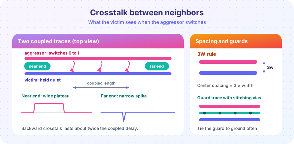
- Backward (near-end) crosstalk flows back toward the aggressor's driver. It appears at the near end as a wide plateau whose duration is about twice the coupled delay and whose amplitude saturates once the coupled length exceeds half the edge's spatial length.
- Forward (far-end) crosstalk travels along with the aggressor's edge and arrives as a narrow spike at the far end. In a stripline surrounded by uniform dielectric it nearly cancels; in a microstrip it does not.
A commonly used estimate for backward crosstalk between microstrips is that the coupling coefficient falls as
Kb ≈ K0 / (1 + (s/h)²)
with s the edge-to-edge spacing and h the height above the plane. It is only an approximation, but it captures the key behavior: spacing relative to height is what matters. Pull the traces apart by about three times the dielectric height and coupling drops by roughly 90 % compared with traces that nearly touch. Bring the plane closer and the same spacing becomes much more effective.
The 3W rule
The widely quoted 3W rule says to keep the center-to-center spacing of traces at three times the trace width, which leaves an edge-to-edge gap of 2W (some designers use 3W edge to edge to be safer). When w ≈ h, that puts the gap at two to three times h, which is where the model above shows coupling dropping to roughly 10 to 20 %. Treat it as a starting point, not a guarantee: for clocks and sensitive analog nets use more, and for slow signals use less.
What actually helps
- Space them out, especially for long parallel runs. Coupling grows with coupled length until it saturates.
- Bring the reference plane closer (thin dielectric between the signal layer and its plane).
- Route adjacent layers at right angles. Orthogonal traces couple very little.
- Add a guard trace between a sensitive net and an aggressor, grounded at both ends and stitched to ground along its length about every λ/20 of the highest frequency of concern. An unstitched or one-end-grounded guard can make things worse by acting as a resonant antenna.
- Reduce the edge rate where speed does not matter. A series resistor on a clock output that is faster than needed costs nothing and calms the board.
Common misconceptions
"Current returns by the shortest geometric path." At high frequency it returns by the path of least inductance, usually directly under the trace, even if that is the long way around the board.
"A guard trace always helps." Only a guard that is grounded at several points does. A floating or single-ended guard can couple noise rather than block it.
"Splitting ground keeps the analog quiet." Splitting a plane forces return currents to detour and adds loop area. Most mixed-signal boards do better with a single solid ground and careful placement.
Try it
First, see how tightly the return current hugs the trace for different dielectric heights.
Press Run (or Ctrl + Enter) to see the result here.
Program input · what you'd type while the program runs
Type the answers before you press Run, one per line. Each time the program reads a line (with input()), it gets the next line from this box.
Now estimate how much crosstalk spacing buys you. Both axes are relative, so only the shape matters.
Press Run (or Ctrl + Enter) to see the result here.
Program input · what you'd type while the program runs
Type the answers before you press Run, one per line. Each time the program reads a line (with input()), it gets the next line from this box.
Last, a small demonstration of why a plane gap hurts. Slide the detour length and watch the loop area and the relative inductance grow. It is a simplified geometric model that treats inductance as proportional to loop area.
Check your understanding
Quick check · 5 questions
of 5 answered You scored / 5 · perfect!
-
1. At high frequency, which path does the return current prefer?
High-frequency return current minimizes loop inductance, which means the smallest loop area: right under the trace. -
2. A trace crosses a slot in its reference plane. What happens?
The return current cannot cross the slot, so it flows around it. The larger loop radiates and picks up more noise. -
3. How does backward crosstalk appear at the near end of the victim?
Backward crosstalk lasts about twice the coupled delay and appears as a plateau at the near end. -
4. Which guard-trace arrangement is recommended?
A guard must be well grounded, with stitching vias along its length, or it can resonate and make coupling worse. -
5. What is the cheapest way to reduce crosstalk and loop area in a stackup?
A thin dielectric holds the field and the return current tightly under the trace, so coupling and loop area both shrink.
Summary
- Current always flows in a loop; at high frequency the return follows the trace on the reference plane.
- Gaps in the plane force detours and enlarge the loop. Do not route fast signals over slots or splits.
- Backward crosstalk is a plateau at the near end, forward crosstalk a spike at the far end.
- Spacing relative to height sets coupling; roughly three times
hcuts it to about 10 % in the simple model. - Guards must be grounded often, and orthogonal routing on adjacent layers is almost free.
Track your progress
Create a free account to tick off lessons and pick up where you left off on any device.
of PCB Design and Prototyping lessons completed