


















Lesson 2 of 45 · Getting Started
What Is a PCB?
Learn what a printed circuit board is, what every feature on it does (traces, pads, vias, mask, silkscreen) and how copper resistance affects a design.
Before 1940 or so, electronic devices were wired by hand: a technician soldered each connection with a piece of wire between metal posts. It was slow, and every unit was slightly different. The printed circuit board replaced the wires with copper lines that are etched onto an insulating sheet. The idea is credited to Austrian engineer Paul Eisler in the 1930s and 1940s, and it made mass production of radios, then computers, then phones possible.
Today a PCB is both a mechanical support and an electrical network. It holds parts firmly and connects them with conductors that are identical on every copy. In this lesson you learn the names of the features you will see on every board, and then you use a first calculation to see why copper geometry matters.
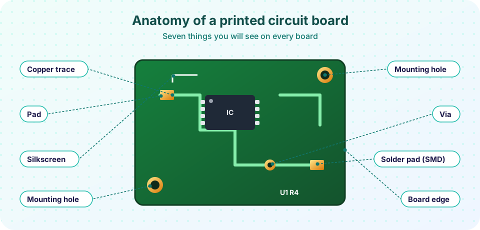
What you will learn
- What a PCB is made of and why each material is used
- The names and jobs of traces, pads, vias, solder mask and silkscreen
- The difference between through-hole and surface-mount construction
- How to estimate the resistance of a copper trace
Key terms
Substrate: the insulating base, most often FR-4 (glass-fiber cloth soaked in epoxy resin).
Trace: a strip of copper that carries a signal or power between pads.
Pad: an exposed copper area where a component lead is soldered.
Via: a small plated hole that connects copper on different layers.
Solder mask: the coloured lacquer (usually green) that covers copper except at pads.
Silkscreen: white ink printed on top for labels and outlines.
The materials
A standard board starts as a sandwich: a sheet of FR-4 with a thin foil of copper bonded to one or both faces. FR-4 is cheap, strong, a good insulator and tolerates soldering temperatures. Its name means "flame retardant, grade 4". It is slightly flexible in thin sheets and very stiff at the usual thickness of 1.6 mm.
Copper is the conductor because it conducts electricity extremely well (resistivity about 1.68 × 10⁻⁸ Ω·m at 20 °C), is easy to etch and solders well. The factory prints a pattern of resist over the foil and dissolves the rest in a chemical bath, so only your traces and pads remain. This is called subtractive etching.
Finally the board is coated with solder mask. The mask does two jobs: it protects the copper from corrosion and it stops solder from flowing along traces and creating shorts. The mask has openings only where you want solder. Silkscreen is printed over the mask so people can read the part names and orientation marks.
The features, one by one
Traces are your wires. Their width decides how much current they can carry (Chapter 4 covers this) and their length affects resistance and delay. A trace on a normal board is a flat rectangle of copper 35 µm thick, and you choose only its width and path.
Pads are the contact points. A through-hole pad has a drilled hole for a lead and is plated inside. A surface-mount pad has no hole; the part sits on top and is soldered to the flat copper.
Vias carry a signal from one layer to another. A via looks like a pad with a small hole. The hole is plated with copper, so the signal passes through the barrel. Unlike a component pad, a via is not meant to hold a lead.
Mounting holes are unplated or plated holes for screws that hold the board in a case. The board outline is the cut path along the edge. It is not copper; it tells the fab where to cut the board from the larger production panel.
Through-hole and surface-mount
Two construction styles share most boards.
- Through-hole (THT) parts have leads that pass through holes and are soldered on the other side. They are strong and easy to solder by hand, which suits connectors, large capacitors and learning projects.
- Surface-mount (SMT) parts sit on the surface and are soldered to pads. They are smaller, cheaper and can be placed by machine at very high speed. Almost all modern consumer electronics are mostly SMT.
Many boards mix both: SMT for most of the circuit and through-hole for connectors that must survive being pulled. You choose per part, and Chapter 3 shows how.
A first calculation: trace resistance
A copper trace is a conductor with a rectangular cross-section, so its resistance follows the standard formula R = ρ × L / (w × t), where ρ is the resistivity in ohm-metres, L the length, w the width and t the thickness, all in metres.
Take a trace 100 mm long, 0.25 mm wide, on 1 oz copper (35 µm). Converted to metres: L = 0.1, w = 0.00025, t = 0.000035. Then R = 1.68e-8 × 0.1 / (0.00025 × 0.000035) = 0.19 Ω (about). That looks small, but it is not negligible: carrying 1 A it would drop 0.19 V and dissipate 0.19 W. Longer and narrower traces make this worse quickly, which is why power traces are wide.
Common misconceptions
"The green colour means something electrical." It does not. Solder mask comes in many colours (red, blue, black, white). Green is common because it was the cheapest and standard for a long time, and it is easy to inspect.
"Traces have zero resistance." They have small but real resistance, inductance and capacitance. On low-current logic you ignore it; on power and fast signals you cannot.
"A via is just a hole." A via is a plated barrel. An unplated hole conducts nothing between layers.
Try it
First, an interactive board. Use the checkboxes to switch the layers on and off, and notice which feature belongs to which layer. This is a demonstration drawing, not a real design.
Second, the resistance of a trace. The code plots how resistance grows with length for three widths. Try changing t to a 2 oz value (70 µm) and see the curves fall.
Press Run (or Ctrl + Enter) to see the result here.
Program input · what you'd type while the program runs
Type the answers before you press Run, one per line. Each time the program reads a line (with input()), it gets the next line from this box.
Check your understanding
Quick check · 5 questions
of 5 answered You scored / 5 · perfect!
-
1. What is FR-4?
FR-4 is the standard substrate: strong, cheap and a good insulator. -
2. What is the job of the solder mask?
The mask covers the copper except at pads; the silkscreen prints the labels. -
3. A via differs from a mounting hole because it is
A plated barrel conducts between layers; a mounting hole is mechanical. -
4. Doubling the width of a trace (same length and copper) does what to its resistance?
R = ρL/(wt), so resistance is inversely proportional to the width. -
5. Which is true of surface-mount parts?
SMT parts sit on pads; mixed boards with through-hole connectors are very common.
Summary
- A PCB is copper on an insulating substrate (usually FR-4) that supports and connects components.
- Traces connect, pads solder, vias join layers, mask protects and silkscreen labels.
- Through-hole and surface-mount parts are often mixed on one board.
- Trace resistance is
R = ρL/(wt); narrow, long traces drop voltage and waste power.
Next: Layers and Materials
Track your progress
Create a free account to tick off lessons and pick up where you left off on any device.
of PCB Design and Prototyping lessons completed