


















Lesson 29 of 45 · Manufacturing and Assembly
How a board is made
Follow a PCB through lamination, drilling, plating, etching, solder mask and surface finish, and learn the design rules (trace, ring, aspect ratio) that each step creates.
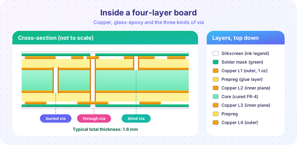
A printed circuit board looks like a single green slab, but it is a sandwich. Sheets of glass-reinforced epoxy and copper foil are pressed together, drilled, plated and etched until the copper that remains is exactly your layout. Every step has a physical limit, and those limits are the design rules you set in your CAD tool.
Knowing the process turns rules from arbitrary numbers into common sense. You will see why a very small drill cannot go through a thick board, why thin traces cost more, and why the copper edge must stay away from the outline.
What you will learn
- Name the layers of a typical four-layer stackup and their purpose.
- Describe lamination, drilling, plating, etching, masking and finishing.
- Calculate annular ring and via aspect ratio and check them against typical limits.
- Choose a surface finish for a given board.
Key terms
Prepreg: glass cloth pre-soaked in uncured epoxy; it melts and bonds layers during lamination.
Core: a fully cured laminate with copper on both sides.
Annular ring: the copper left around a drilled hole, (pad diameter − drill diameter) / 2.
Aspect ratio: board thickness divided by drill diameter.
Surface finish: the metal coating on exposed pads that protects copper and aids soldering (HASL, ENIG, OSP).
From laminate to bare board
- Inner layers. A core with copper on both sides is coated with photoresist, exposed through a film (or by laser) of your layout, developed, and etched. Chemistry removes the unprotected copper and leaves traces.
- Lamination. Inner cores and prepreg sheets are stacked with outer copper foil and pressed under heat and vacuum. The prepreg flows and cures into a solid board. A standard finished thickness is 1.6 mm.
- Drilling. CNC drills punch the holes for vias and through-hole parts. Very small holes (below about 0.2 mm) are drilled by laser or require more expensive processes.
- Plating. The hole walls are glass and epoxy, not metal. A thin chemical copper layer makes them conductive and electroplating builds it up (about 20 to 25 µm) so each hole becomes a barrel that connects layers.
- Outer layers. Photoresist is applied again, the pattern exposed, copper plated on the traces, a protective metal applied, and the rest etched away.
- Solder mask. A green (or any color) polymer covers everything except the pads, protecting copper and preventing solder bridges.
- Surface finish and silkscreen. Exposed pads receive their finish, then ink prints legends.
- Profile and test. Boards are routed or scored out of the panel and electrically tested for shorts and opens (flying probe or fixture).
Via types
| Via | Connects | Cost |
|---|---|---|
| Through | Top to bottom, all layers | Lowest |
| Blind | An outer layer to one or more inner layers | Higher (sequential lamination or laser) |
| Buried | Inner layers only | Higher |
| Microvia | Adjacent layers, laser-drilled | Higher, needed for fine-pitch BGAs |
Start with through vias; add blind or buried vias only when density demands it.
Where the design rules come from
- Trace width and spacing. Etching undercuts the sides of a trace slightly, so very thin copper at a tight pitch is harder to control. Low-cost fabs typically handle 0.15 mm (6 mil) trace and space; finer rules cost more.
- Annular ring. The drill wanders by a small tolerance, so the pad must be larger than the hole by enough to keep copper all around it. A pad of 0.6 mm around a 0.3 mm hole leaves
(0.6 − 0.3)/2 = 0.15 mm, a common minimum. - Aspect ratio. Plating solution must reach the bottom of the hole. A 1.6 mm board with a 0.2 mm drill has an aspect ratio of 8:1, around the usual limit of 8:1 to 10:1 for economical fabs.
- Copper weight. 1 oz is 35 µm and is standard on outer layers. Heavier copper carries more current but needs wider spacing, because etching a thick layer undercuts more.
- Edge clearance. Routing the board outline has a tolerance, so copper must stay about 0.3 mm from the edge to avoid being exposed.
Surface finishes
| Finish | Strengths | Watch for |
|---|---|---|
| HASL (lead-free or leaded) | Cheap, solderable, easy hand soldering | Uneven surface, poor for fine pitch |
| ENIG (nickel and gold) | Flat, long shelf life, good for fine pitch and BGAs | Higher cost; avoid thick nickel/black pad defects |
| OSP | Cheap, flat | Short shelf life, one reflow pass preferred |
| Immersion silver / tin | Flat, good for RF | Tarnish handling |
Common misconceptions
"Smaller vias are always better." Smaller drills raise cost and risk, and a high aspect ratio can leave voids in the barrel.
"The solder mask is just color." It defines which copper is exposed. Mask openings that are too small leave a thin copper rim on pads, too big and they expose neighboring traces.
"Heavy copper is always safer." It needs wider spacing and costs more. Use it where current demands it.
Try it
Press Run (or Ctrl + Enter) to see the result here.
Program input · what you'd type while the program runs
Type the answers before you press Run, one per line. Each time the program reads a line (with input()), it gets the next line from this box.
Etching removes a little copper from the sides of every trace. This plot shows how a width variation changes impedance. It uses the IPC-2141 approximation from Chapter 5.
Press Run (or Ctrl + Enter) to see the result here.
Program input · what you'd type while the program runs
Type the answers before you press Run, one per line. Each time the program reads a line (with input()), it gets the next line from this box.
Check your understanding
Quick check · 5 questions
of 5 answered You scored / 5 · perfect!
-
1. What is the annular ring for a 0.8 mm pad around a 0.4 mm drill?
(0.8 − 0.4) / 2 = 0.2 mm. -
2. What is the aspect ratio of a 0.25 mm drill through a 1.6 mm board?
1.6 / 0.25 = 6.4. -
3. Which layer glues inner cores together during lamination?
Prepreg flows and cures under heat and pressure, bonding layers. -
4. Which finish is flat, has a long shelf life and suits fine-pitch BGAs?
ENIG gives a flat, durable surface, which is ideal for fine pitch. -
5. Why must copper stay about 0.3 mm from the board edge?
Profile routing has tolerance, so a margin prevents exposed or torn copper.
Summary
- A board is a lamination of cores, prepreg and copper that is drilled, plated, etched and coated.
- Vias are through, blind, buried or micro; through vias are cheapest.
- Annular ring, aspect ratio, trace and space and edge clearance come directly from process limits.
- Surface finish should match pitch, assembly method and storage time.
Track your progress
Create a free account to tick off lessons and pick up where you left off on any device.
of PCB Design and Prototyping lessons completed