


















Lesson 9 of 45 · From Schematic to Board
Board Setup, Stack-up and Design Rules
Set up a PCB before routing: board outline, layer count, stack-up and design rules for trace width, clearance, via size and annular ring, taken from your fab.
Before you place a single part, tell your layout software about the board you intend to build. This setup is a contract between you and the factory. If your traces are thinner than the factory can etch, or your holes smaller than it can drill, the board will not be made, or it will fail in use. The factory publishes its limits as "capabilities". You copy them into your tool as design rules, and the tool then warns you the moment you break one.
What you will learn
- How to draw the board outline and mounting holes
- How to choose the layer count and import a fab's stack-up
- The main design rules and sensible starting values
- How DRC uses these rules
Key terms
Clearance: the minimum gap between two copper objects of different nets.
Annular ring: the ring of copper left around a drilled hole after drilling.
Drill size: the finished hole diameter of a via or through-hole pad.
Net class: a group of nets that share rules (for example Power with wider traces).
Edge clearance: the minimum distance from copper to the board edge.
The board outline
The outline is a closed shape on a special layer, often called Edge.Cuts. It tells the fab where to cut. Beginners usually start with a rectangle sized to the case or the largest part they must fit, plus a margin. Round the corners with a radius (2 mm is common): square corners are fragile and snag.
Add mounting holes where your enclosure needs screws. For M3 screws, a 3.2 mm hole is a typical clearance hole, and you keep copper and parts away from the area around it. The edge connector or USB socket should be placed so that it overhangs the edge by the right amount; the datasheet usually says how.
Cost scales with area, so a smaller board is cheaper. But do not shrink the board so much that it forces a crowded layout. Leave 10 to 20 percent free space on a first design.
Layers and stack-up
Choose two layers for simple, slow circuits and four layers for faster or denser ones, as Chapter 1 explained. In your CAD tool, open the board setup and set the number of copper layers. Enter the stack-up the fab will use, including copper thicknesses and dielectric thicknesses, because later you will compute trace impedance and plane spacing from it. Most low-cost fabs publish a standard four-layer stack-up for 1.6 mm boards; use theirs.
The design rules
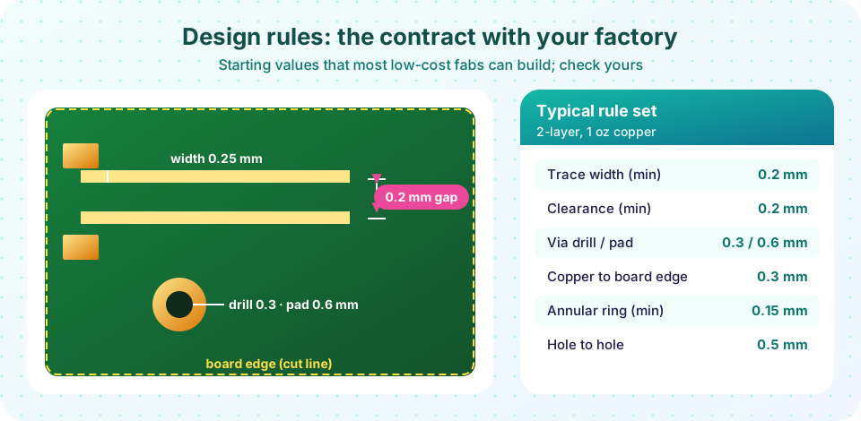
These are the rules every project sets first. The numbers below are typical safe starting points for a two-layer board with 1 oz copper at a low-cost fab. Read your fab's own capability page and use its numbers; they differ and change over time.
| Rule | Typical safe value | What it protects |
|---|---|---|
| Minimum trace width | 0.2 mm (8 mil) | Etching accuracy |
| Minimum clearance | 0.2 mm (8 mil) | Short circuits between nets |
| Via drill / pad | 0.3 mm / 0.6 mm | Drilling and plating |
| Annular ring | 0.15 mm or more | Drill wander cutting the pad |
| Copper to board edge | 0.3 mm or more | Routing/cutting tolerance |
| Hole to hole | 0.5 mm or more | Board strength |
Most fabs can do finer (0.127 mm or 5 mil) at higher cost or with advanced options. A good approach: use comfortable rules where possible and go tight only where needed, for example under a fine-pitch chip. A wider trace is easier to etch, so it is more reliable, and wider spacing is safer at high voltage.
The annular ring follows from geometry: ring = (pad diameter − drill diameter) / 2. For a 0.6 mm pad and 0.3 mm drill, the ring is 0.15 mm. Drills wander slightly, so the ring has to be large enough that the hole stays inside the pad.
Net classes let you set different rules for different groups. A Power class might use 0.5 mm traces and larger vias; the default class uses 0.25 mm. Assign nets to classes once, and the router and DRC follow.
What DRC does
The design rule check measures every distance on the finished board and flags anything smaller than your rules: traces too close, copper too near the edge, drill holes too small, unconnected nets, even silkscreen over pads. Run it often, not only at the end. A DRC with zero errors does not mean the board is good; it means the board obeys the rules you set. If you set the rules badly, a "clean" DRC means nothing.
Common misconceptions
"Set the rules at the end, when I know what I need." Rules affect routing from the first trace. Set them at the beginning.
"Smaller is always better." Tight rules cost money and cut yield. Use the biggest values that fit.
"DRC proves my design works." It checks geometry only. Electrical behavior is your job.
Try it
The first example is a checker that compares a design to a fab's limits and lists violations. The limits are the typical values from the table; replace them with your fab's.
Press Run (or Ctrl + Enter) to see the result here.
Program input · what you'd type while the program runs
Type the answers before you press Run, one per line. Each time the program reads a line (with input()), it gets the next line from this box.
The second example is a live drawing. Move the sliders to change the trace width and the gap between two traces, and see whether the layout passes a 0.2 mm limit.
Check your understanding
Quick check · 5 questions
of 5 answered You scored / 5 · perfect!
-
1. What is an annular ring?
It is the copper between the drill edge and the pad edge. -
2. A via has a 0.6 mm pad and a 0.3 mm drill. What is the annular ring?
(0.6 − 0.3) / 2 = 0.15 mm. -
3. When should you set the design rules?
Rules guide routing from the first trace. -
4. What does a clean DRC prove?
DRC checks geometry against rules, nothing more. -
5. What is a net class used for?
For example, power nets can be wider than signals.
Summary
- Draw the outline, mounting holes and choose layers before placing parts.
- Copy the fab's stack-up and capabilities into your design rules.
- Typical starting values: 0.2 mm trace and clearance, 0.3 mm drill with 0.6 mm pad.
- DRC checks geometry against your rules, so the rules must be right.
Next: Chapter 2 Review
Track your progress
Create a free account to tick off lessons and pick up where you left off on any device.
of PCB Design and Prototyping lessons completed