


















Lesson 17 of 45 · Layout and Routing
Chapter 4 Overview: Layout and Routing
Overview of chapter 4: part placement, trace width and current, vias, and ground planes with return paths, the four habits behind a good board layout.
Layout is the stage most people imagine when they think of PCB design: parts on the board, copper lines between them. It is also where a circuit that was fine on paper can fail in practice. The same schematic can become a quiet, reliable board or a noisy, hot, unstable one depending on where you put things and how you route them.
In this chapter you will learn the four decisions that matter most: where to place parts, how wide to make traces, when and how to use vias, and how to keep a clean return path for every signal.
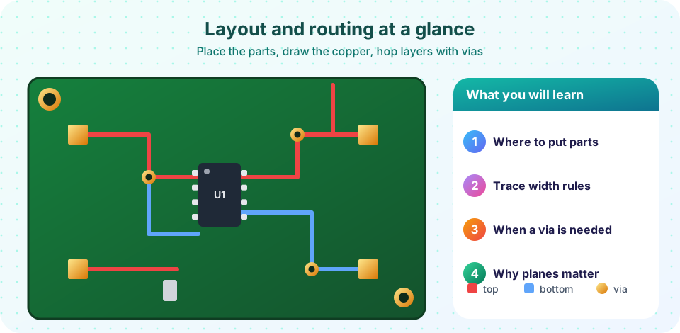
Layout in order
Placement
Traces
Vias
Return paths
What you will learn in this chapter
- How to group and place parts so that routing is short and clean
- How to calculate a trace width from current and temperature rise
- What vias cost in resistance, inductance and money
- Why every signal needs a return path and how ground planes provide one
The lessons
- Placement Strategy: zones, connectors, decoupling and crystals.
- Trace Width and Current: IPC-2221 and the resistance of copper.
- Vias and Layer Changes: types of via, sizes and what a via adds.
- Ground Planes and Return Paths: why loops matter.
- Chapter 4 Review: recap and quiz.
A good order of work
A well-organised layout session follows a sequence.
- Board outline, mounting holes and fixed parts first. Connectors, switches, LEDs and anything that touches a case are fixed by mechanics.
- Place the important parts next. The processor, then the parts that connect to it most tightly: decoupling capacitors, the crystal, the power input and regulator.
- Place the rest in groups. Keep each functional block together.
- Route the critical nets first: power, then fast or sensitive signals, then the rest. Do not let a router or the first free path decide them.
- Add planes and stitching. Fill ground and, where used, power areas.
- Clean up: silkscreen, test points, 3D check, DRC.
Throughout, use the airwires (ratsnest). If lines crowd at one point, move parts. If a part will be hard to solder, move it. Good placement makes routing nearly trivial; bad placement cannot be fixed by clever routing.
Check your understanding
Quick check · 3 questions
of 3 answered You scored / 3 · perfect!
-
1. Which should be placed first on most boards?
Mechanical constraints fix connectors and mounting points. -
2. What is the ratsnest?
Airwires show what still needs copper. -
3. Which nets are usually routed first?
Critical nets need the best paths.
Summary
- Layout follows a sequence: fixed parts, key parts, groups, critical nets, planes, cleanup.
- Placement quality decides routing quality.
- The next lessons cover placement, trace width, vias and return paths.
Next: Placement Strategy
Track your progress
Create a free account to tick off lessons and pick up where you left off on any device.
of PCB Design and Prototyping lessons completed