


















Lesson 38 of 45 · Complete Projects
Project: a USB-C powered sensor board
Design a small two-layer USB-C sensor board: CC resistors, ESD protection, LDO power dissipation, decoupling, I2C pull-ups, USB routing, floorplan and test points.
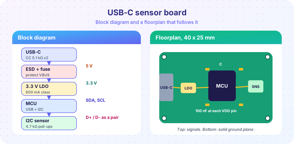
The goal: a 40 × 25 mm board that plugs into any USB-C port, powers itself from 5 V, reads a temperature and humidity sensor over I2C, and reports the data to a computer over USB. It is a typical "first real board": a connector, a regulator, a microcontroller, a sensor, and a handful of passives.
You will make each decision with a calculation or a rule from earlier chapters, and finish with a floorplan, a stackup and a pre-order checklist.
What you will learn
- Choose the USB-C resistors and protection for a simple sink device.
- Calculate LDO dissipation and temperature rise.
- Size I2C pull-up resistors from bus capacitance and rise time.
- Decide trace widths and routing for a two-layer board.
Key terms
Sink: a device that receives power from the USB port.
CC1/CC2: configuration pins; a 5.1 kΩ resistor to ground on each tells a source that a sink is attached and requests default power.
LDO: low-dropout linear regulator; it burns (Vin − Vout)·I as heat.
Pull-up resistor: a resistor from an open-drain bus line to the supply.
TVS / ESD diode: a clamp that absorbs voltage spikes.
Requirements
| Item | Value |
|---|---|
| Input | USB-C, 5 V, default USB power (a USB 2.0 port allows up to 500 mA) |
| Output | 3.3 V for MCU and sensor, about 50 mA |
| Interface | USB 2.0 full speed (12 Mb/s) to a computer |
| Bus | I2C at 400 kHz to a sensor |
| Size | 40 × 25 mm, two layers, 1.6 mm FR-4 |
Power input and protection
A USB-C sink for USB 2.0 only needs the VBUS, GND, D+, D−, CC1, CC2 and shield pins. Put 5.1 kΩ from each CC pin to ground; that is how the source recognizes a sink. Connect all ground pins and the shield to ground (some designs use a resistor and capacitor in parallel for the shield).
Add protection close to the connector, in this order along the power path: a small fuse or PTC (or a current-limit switch), a TVS diode to ground, then bulk capacitance. On the data lines add a low-capacitance ESD diode array right at the connector pins. Cable plugging is the harshest event your board will see.
The LDO: where the heat goes
A linear regulator turns every volt of drop into heat: P = (Vin − Vout) · Iout. At 5 V → 3.3 V and 50 mA that is 85 mW; at 150 mA it is 255 mW. With a small package having θJA ≈ 200 °C/W, a 255 mW load raises the junction by about 51 °C, which is acceptable at room temperature but not in a hot enclosure. A switching regulator (project 2) avoids the problem when the current is large.
Follow the datasheet's capacitor recommendation (typically 1 µF at the input and 1 to 10 µF at the output, low-ESR ceramic parts; some LDOs are unstable with the wrong ESR). Keep these capacitors adjacent to the LDO pins with a short ground return.
Microcontroller essentials
- 100 nF per VDD pin, placed at the pin; one 4.7 to 10 µF bulk capacitor nearby (the chapter-5 recipe).
- Reset pull-up and an optional button; boot pin states per datasheet.
- Debug header: SWD (3.3 V, GND, SWDIO, SWCLK, optional reset) on 1.27 mm pads or tag-connect footprint.
- Crystal (if used): load capacitors matched to the crystal spec (including stray capacitance), short traces, no routing beneath it.
I2C pull-ups
I2C lines are open-drain. The bus capacitance Cb and the pull-up Rp form an RC that sets the rise time: tr ≈ 0.8473 · Rp · Cb. Fast mode (400 kHz) allows at most 300 ns, so Rp ≤ 300 ns / (0.8473 · Cb). The pull-up must also be low enough that a device can sink the current: Rp ≥ (VDD − 0.4 V) / 3 mA. With Cb = 100 pF: Rp ≤ 3.5 kΩ; the lower limit at 3.3 V is about 970 Ω. A 2.2 kΩ to 3.3 kΩ pair is a good choice here (4.7 kΩ is the classic value for 100 kHz buses with lower capacitance).
USB data and a two-layer stackup
USB 2.0 full speed has edges of 4 to 20 ns, so the traces from the connector to the MCU (a couple of centimeters) are short compared with the edge: they behave as lumped wires and do not need exact 90 Ω differential impedance. (High-speed 480 Mb/s USB does need it.) Still, route D+ and D− together as a pair, equal length within a few millimeters, over solid ground, with no stubs.
On a two-layer board the dielectric between the top trace and the bottom ground plane is the full 1.6 mm. That makes a 50 Ω microstrip about 3 mm wide (the IPC-2141 formula gives about 2.99 mm), which is why two-layer boards rarely achieve controlled impedance on narrow traces. For this project you do not need to: keep fast traces short and use a solid ground pour on the bottom layer, with stitching vias where the pour is cut by signals.
Placement and routing priorities
- Connector on the board edge; fuse, TVS and bulk capacitor next to it.
- LDO near the connector; short, wide power traces (0.5 mm or more for 100 mA, easily met).
- MCU in the middle with its decoupling at the pins.
- Sensor away from the LDO and the MCU's hottest side so it measures air, not the board; cut slots in the board around it only if needed.
- Route USB first, then I2C, then everything else; power by pour and wide traces.
- Place test points: 5 V, 3.3 V, GND (two), RESET, SDA, SCL.
Common misconceptions
"USB-C always means fast charging." A sink with 5.1 kΩ CC resistors gets default 5 V power, not fast charging. Higher power needs a PD controller.
"I2C pull-ups can be anything." Too large and the bus is slow; too small and devices cannot pull it low.
"The LDO is a free lunch." It is cheap and quiet, but all the drop becomes heat.
Try it
Press Run (or Ctrl + Enter) to see the result here.
Program input · what you'd type while the program runs
Type the answers before you press Run, one per line. Each time the program reads a line (with input()), it gets the next line from this box.
Press Run (or Ctrl + Enter) to see the result here.
Program input · what you'd type while the program runs
Type the answers before you press Run, one per line. Each time the program reads a line (with input()), it gets the next line from this box.
Press Run (or Ctrl + Enter) to see the console output here.
No output.
Check your understanding
Quick check · 5 questions
of 5 answered You scored / 5 · perfect!
-
1. What do the 5.1 kΩ resistors on the CC pins do?
5.1 kΩ to ground on CC1 and CC2 identifies a sink. -
2. An LDO drops 5 V to 3.3 V at 100 mA. How much power does it dissipate?
(5 − 3.3) V × 0.1 A = 0.17 W. -
3. What is the maximum pull-up for a 400 kHz I2C bus with 100 pF bus capacitance?
300 ns / (0.8473 × 100 pF) ≈ 3.54 kΩ. -
4. Why is controlled-impedance routing hard on a two-layer board?
With 1.6 mm to the plane, the width for 50 Ω is about 3 mm. -
5. Why is USB 2.0 full speed tolerant of short uncontrolled traces?
The edge (4 to 20 ns) is much longer than the delay of a few centimeters.
Summary
- Use 5.1 kΩ on each CC pin, protection at the connector, and decoupling at every power pin.
- LDO heat is
(Vin − Vout)·I; check temperature rise. - Choose I2C pull-ups between about 1 kΩ and
tr/(0.8473·Cb). - On two layers, keep fast traces short over a solid ground pour.
Next: Buck regulator board
Track your progress
Create a free account to tick off lessons and pick up where you left off on any device.
of PCB Design and Prototyping lessons completed