


















Lesson 44 of 45 · Projects and Practice
Cheat sheet: PCB design formulas on one page
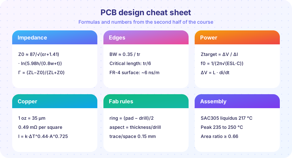
A one-page PCB design cheat sheet: impedance, reflections, edge speed, decoupling, copper, fabrication rules and reflow numbers, with typical values and a bring-up order.
When you are in the middle of a layout you do not want to reread five lessons. You need the formula, the typical value and the rule of thumb, in one place. This page collects them. Print it, pin it above the bench, and retrace the formulas in the lessons linked at the end.
What you will learn
- Find the right formula or number quickly.
- Recall typical limits for fabrication and assembly.
- Use a one-page review before you order.
Key terms
Z0, Γ: characteristic impedance and reflection coefficient.
tr, BW: rise time and bandwidth.
ESL, C, Ztarget: capacitor inductance, capacitance and target impedance.
ΔT, A, I: temperature rise, copper cross-section (mil²) and current (A).
Formulas
Signals
| Quantity | Formula or rule |
|---|---|
| Microstrip impedance | Z0 ≈ 87/√(εr+1.41) · ln(5.98h/(0.8w+t)), valid for 0.1 < w/h < 2 |
| Reflection | Γ = (ZL − Z0)/(ZL + Z0) |
| Series termination | Rs = Z0 − Rdriver |
| Bandwidth from edge | BW ≈ 0.35 / tr |
| Delay on FR-4 | about 6 ns/m on a surface trace, 7 ns/m in an inner stripline |
| Critical length | one-way delay greater than tr/6 to tr/4 |
Return current within ±x |
(2/π)·atan(x/h) |
| Crosstalk | falls roughly as 1/(1+(s/h)²); 3W center spacing as a start |
Power
| Quantity | Formula or rule |
|---|---|
| Voltage spike | ΔV = L · di/dt |
| Capacitor self-resonance | f0 = 1/(2π√(ESL·C)) |
| Target impedance | Ztarget = ΔV / ΔI |
| Plane capacitance | C = ε0·εr·A/d |
| LDO heat | P = (Vin − Vout)·I |
| Buck | D = Vout/Vin; ΔIL = (Vin − Vout)·D/(L·fsw); Icin,rms = Iout·√(D(1−D)) |
| Ring frequency | f = 1/(2π√(L·C)) |
Copper and fabrication
| Quantity | Value |
|---|---|
| 1 oz copper | 35 µm thick; about 0.49 mΩ per square at 20 °C |
| IPC-2221 current | I = k·ΔT^0.44·A^0.725 (A in mil²; k = 0.048 outer, 0.024 inner) |
| Annular ring | (pad − drill)/2, at least about 0.15 mm |
| Via aspect ratio | thickness / drill ≤ about 8 to 10 |
| Low-cost trace/space | about 0.15 mm (6 mil) |
| Edge clearance | about 0.3 mm |
Assembly and test
| Quantity | Value |
|---|---|
| Stencil | 0.10 to 0.13 mm; area ratio ≥ 0.66; aspect ratio ≥ 1.5 |
| SAC305 | liquidus 217 °C; peak 235 to 250 °C; 30 to 90 s above liquidus |
| Hand soldering | iron about 320 to 350 °C (lead-free), 2 to 3 s per joint |
| Bring-up order | inspect, ohms to GND, current limit, rails, clock/reset, SWD, firmware |
| Test access | pads about 1 mm, 2.5 mm apart, 90 % of nets |
| EMC | E ∝ f²·A·I: halve the loop = −6 dB; double the frequency = +12 dB |
Topic map
Signals: impedance, crosstalk, decoupling. Manufacturing: fabrication, files, assembly. Test: bring-up, DFM, DFT, EMC. Projects: USB-C, buck.
Common misconceptions
"The cheat sheet replaces understanding." It only reminds you. Always check a formula's validity range.
"Typical values are limits." Fabs and parts differ; read the datasheet and the fab's capability page.
Try it
Press Run (or Ctrl + Enter) to see the result here.
Program input · what you'd type while the program runs
Type the answers before you press Run, one per line. Each time the program reads a line (with input()), it gets the next line from this box.
Check your understanding
Quick check · 4 questions
of 4 answered You scored / 4 · perfect!
-
1. Which formula gives the bandwidth of an edge?
A rise time of 1 ns means about 350 MHz. -
2. What is the IPC-2221 constant k for inner layers?
k = 0.048 for outer layers and 0.024 for inner. -
3. Which is the correct order for bring-up?
Safe, cheap checks first. -
4. SAC305 reaches full liquid at about:
The liquidus is about 217 °C.
Summary
- One page of formulas covers signals, power, copper, fabrication, assembly and test.
- Check validity ranges and datasheets before trusting any number.
Next: Further study
Track your progress
Create a free account to tick off lessons and pick up where you left off on any device.
of PCB Design and Prototyping lessons completed