


















Lesson 20 of 45 · Layout and Routing
Vias and Layer Changes
Learn about PCB via types (through, blind, buried, micro), sizes and annular ring, via resistance and inductance, tenting, thermal vias and when to change layers.
A via is how a trace changes layers. Without vias, every connection would have to stay on one layer and could never cross another. With vias, a router can hop over an obstacle, reach a ground plane or carry a signal from the top side to the bottom. Vias are so common that a dense board may have thousands.
Vias are not free. Each one takes space, costs a little in manufacturing, adds resistance and inductance and breaks the nearby return path. This lesson shows how they are built, how to size them and how to use them wisely.
What you will learn
- The four via types and when each is used
- How to choose drill and pad size, and what the aspect ratio limits
- The resistance and inductance of a via
- Practical rules: stitching, thermal vias, tenting and via-in-pad
Key terms
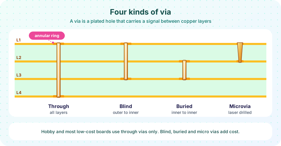
Through via: drilled through the whole board and plated; connects any layers.
Blind via: starts on an outer layer and ends on an inner one.
Buried via: connects inner layers only; invisible from outside.
Microvia: a tiny laser-drilled via, usually spanning one layer pair.
Aspect ratio: board thickness divided by drill diameter; fabs limit it (commonly about 8:1 to 10:1 for standard processes).
Tenting: covering a via with solder mask so it is closed.
How a via is made
The factory drills a hole through the laminated board. It then plates the hole walls with copper, typically 20 to 25 µm thick, in a chemical and electrical process. This copper tube, called the barrel, joins the copper on every layer that the hole touches. Each layer has a pad around the hole called the annular ring, which must be large enough that a slightly off-centre drill still leaves copper all round.
Common sizes on low-cost boards: drill 0.3 mm with a pad 0.6 mm, giving a ring of 0.15 mm. Smaller vias (0.2 mm drill and 0.45 mm pad) are available at higher cost. For power or hand-soldering, 0.4 mm drill with a 0.8 mm pad is easier and sturdier.
The aspect ratio limits how small a via can be in a thick board. A 1.6 mm board with 0.3 mm drills has a ratio of 1.6 / 0.3, about 5.3, which is easy. A 0.1 mm drill would need a ratio of 16:1, which is not possible for mechanical drilling, so very small vias use lasers and thin layers.
The types of via
- Through vias are the cheapest and most common. Their only drawback is the stub on layers you do not use, and the space they take on all layers.
- Blind and buried vias are made by drilling and plating sub-stacks before pressing the board together. They free space on other layers, but each extra step adds cost, sometimes a large fraction of the board price.
- Microvias connect adjacent layers and let a BGA with 0.5 mm pitch break out. They are part of HDI (high-density interconnect) design and need an advanced fab.
For a hobby or a first product, use through vias only. If you need blind or buried vias, you probably have a dense product, and you should talk to the factory first.
What a via adds
Resistance. A plated barrel is a thin tube of copper. Its cross-section area is about π × (D − t) × t, where D is the drill diameter and t the plating thickness. For a 0.3 mm drill with 25 µm plating that is π × 0.275 mm × 0.025 mm, or about 0.0216 mm². The barrel of a 1.6 mm board then has R = ρL/A = 1.68e-8 × 1.6e-3 / 2.16e-8 = 1.2 mΩ. That is small, but a few amperes through one via heat it. Use several vias in parallel for power, a good rule is at least one via per ampere or so and check the manufacturer's data for the exact limit.
Inductance. The barrel behaves like a short wire. A widely used approximation is L ≈ 5.08 × h × (ln(4h/d) + 1) nH, with h (length) and d (diameter) in inches. For a 1.6 mm (0.063 in) via with a 0.3 mm (0.0118 in) drill this gives about 1.3 nH. That matches the rule of 1 nH per millimetre. It matters for decoupling and fast signals: a via is a small inductor in series.
Return path disturbance. When a signal changes layer, its return current must also change reference planes. If both planes are the same ground, put a ground via beside the signal via so the return can jump too (stitching). For fast edges this is important; for slow ones it is not.
Practical habits
- Via near the pad, not in it. A via in the pad of a surface-mount part lets solder flow down the hole and starve the joint. If you must use via-in-pad, ask the fab to fill and cap them (extra cost).
- Tent small vias with mask on the board's side that gets assembled so solder does not wick in. Many fabs tent by default; check the rule. Leave test vias open.
- Thermal vias: under a QFN or power part, a grid of vias (for example 0.3 mm drills at 1 mm spacing) carries heat to a copper pour on another layer. Paste can run into them, so fabs fill or tent them.
- Keep one signal's vias few. Each layer change is a small discontinuity. Prefer a route that stays on one layer.
- Don't put vias on pads of 0402 or smaller unless needed, and keep vias away from the board edge.
- Use the right net rule. Make a via class for power (0.4 / 0.8 mm) and one for signals (0.3 / 0.6 mm).
Common misconceptions
"A via is a perfect wire." It has resistance, inductance and parasitic capacitance. At high speed or high current, you must count them.
"One via is enough for power." One via carries limited current. Use several in parallel.
"Blind vias are just better vias." They are more expensive and only needed for dense designs. Through vias are fine for most boards.
Try it
The first example computes resistance and a rough current limit for vias of different sizes. The current limit uses the IPC-2221 area formula for the barrel's cross-section on an internal layer (k = 0.024), so it is conservative. Edit the drill and plating values.
Press Run (or Ctrl + Enter) to see the result here.
Program input · what you'd type while the program runs
Type the answers before you press Run, one per line. Each time the program reads a line (with input()), it gets the next line from this box.
The second example plots via inductance against board thickness using the approximation above, for three drill sizes. Notice how weakly the drill diameter matters and how strongly the board thickness matters.
Press Run (or Ctrl + Enter) to see the result here.
Program input · what you'd type while the program runs
Type the answers before you press Run, one per line. Each time the program reads a line (with input()), it gets the next line from this box.
Check your understanding
Quick check · 5 questions
of 5 answered You scored / 5 · perfect!
-
1. Which via type connects an outer layer to an inner layer only?
A blind via starts on an outside layer and ends inside the board. -
2. A 1.6 mm board has 0.3 mm drills. What is the aspect ratio?
1.6 / 0.3 ≈ 5.3, easy for standard fabs. -
3. What does a ground via next to a signal via help with?
Stitching vias let the return current follow the signal. -
4. Why is via-in-pad risky without special processing?
Open vias in pads wick solder; fill and cap them if you must. -
5. About what inductance does a via through a 1.6 mm board have?
Around 1.3 nH from the common approximation, matching 1 nH per millimetre.
Summary
- Vias are plated holes; through vias are cheapest, blind, buried and micro vias cost more.
- Typical sizes: 0.3 mm drill with a 0.6 mm pad; mind the annular ring and aspect ratio.
- A via has about 1 mΩ resistance and about 1 nH inductance on a 1.6 mm board.
- Use parallel vias for power, stitching vias beside fast signals and avoid via-in-pad unless filled.
Track your progress
Create a free account to tick off lessons and pick up where you left off on any device.
of PCB Design and Prototyping lessons completed