


















Lesson 22 of 45 · Layout and Routing
Chapter 4 Review: Layout and Routing
Review placement, trace width and current, vias and return paths with a recap table, a one-picture summary and a ten-question quiz for chapter 4.
You have now seen the full path from a blank board to routed copper. This chapter gave you four habits: place parts in groups with short loops, size traces from current, use vias deliberately and keep a solid return path under every signal. Most good layouts are those four habits repeated carefully.
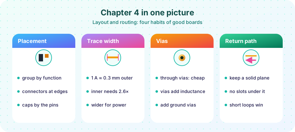
Recap table
| Topic | Remember |
|---|---|
| Placement | Fixed parts first; zones; connectors at edges; decoupling at pins; crystal next to chip |
| Trace inductance | About 1 nH per mm; 10 mm of detour adds more than 6 Ω at 100 MHz |
| Trace width | I = k·ΔT^0.44·A^0.725; 1 A needs about 0.3 mm outer, 0.78 mm inner (1 oz, 10 °C) |
| Voltage drop | R = ρL/(wt); keep rail drop below 1 to 2 % |
| Vias | Through, blind, buried, micro; 0.3/0.6 mm; about 1 mΩ and 1 nH on a 1.6 mm board |
| Via habits | Parallel vias for power; avoid via-in-pad; stitch ground at layer changes |
| Return path | Small loops; current follows the trace in the plane; no slots under signals |
Lessons in this chapter
Check your understanding
Quick check · 10 questions
of 10 answered You scored / 10 · perfect!
-
1. What is the best place for a decoupling capacitor?
A short loop keeps the inductance low. -
2. A 20 mm trace detour adds roughly how much inductance (1 nH/mm)?
20 mm × 1 nH/mm = 20 nH. -
3. For 2 A at a 10 °C rise on 1 oz copper, an outer trace needs about
IPC-2221 gives about 0.78 mm for 2 A on an outer layer. -
4. Which has the greater effect on required width: current or copper weight?
Width scales about as I^1.38 and inversely with thickness. -
5. Which via type connects an outer layer to an inner layer only?
Blind vias end inside the board. -
6. A via with a 0.7 mm pad and 0.4 mm drill has an annular ring of
(0.7 − 0.4) / 2 = 0.15 mm. -
7. Why use several vias in parallel for a power connection?
Parallel vias share current and reduce resistance and inductance. -
8. A signal crosses a slot in the plane. The return current
The detour creates a big loop that radiates and picks up noise. -
9. How much of the return current lies within ±h of the trace over an ideal plane at height h?
(2/π)·arctan(1) = 50 %. -
10. What is the best way to separate analog and digital circuits?
Placement separation avoids cutting return paths.
Summary
- Place by function with short loops and key parts first.
- Size power traces from current, temperature rise and voltage drop.
- Use through vias by default, in parallel for current, with ground stitching beside signals.
- Keep a solid plane under signals and avoid slots; loop area is the enemy.
Next: continue with the rest of the course on the PCB Design and Prototyping track page.
Track your progress
Create a free account to tick off lessons and pick up where you left off on any device.
of PCB Design and Prototyping lessons completed