


















Lesson 35 of 45 · Testing and Debugging
DFM, DFT and EMC
Learn design-for-manufacture, design-for-test and EMC habits for PCBs: rule margins, fiducials, test points, headers, loop area, filtering and pre-compliance checks.
Some design decisions are invisible until later. A pad that is 0.1 mm too small will still look right in your CAD tool, but will tombstone in the oven. A rail with no test point will cost you an hour with a hot-air gun and a fine probe. A clock loop that is twice as large as it needs to be will pass the functional test and fail the emissions test months later.
Three habits address these: design for manufacture (DFM), design for test (DFT) and EMC awareness. They cost almost nothing while you are laying out the board, and they cost a lot to retrofit.
What you will learn
- Apply DFM margins and avoid common assembly traps.
- Add test points and a programming header with sensible placement.
- Explain why loop area and edge rate drive emissions.
- Use filters, ground and shielding basics to reduce EMI.
Key terms
DFM: design for manufacture; layouts that are easy to build reliably.
DFT: design for test; layouts that are easy to verify.
Fiducial: a copper mark that lets the placement machine find the board's position.
EMC / EMI: electromagnetic compatibility and interference: emissions from and immunity of your product.
Common-mode current: current flowing in the same direction on a cable's conductors, which is the main cause of radiated emissions from cables.
Design for manufacture
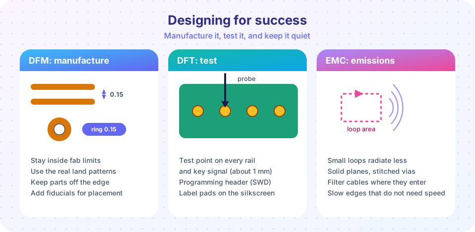
- Design with margin. If the fab's minimum is 0.15 mm, design for 0.2 mm where space allows. Yield and price both improve.
- Use the manufacturer's land patterns for parts, or IPC-7351 families, and keep pads symmetric to avoid tombstoning. Connect small pads to copper symmetrically.
- Add fiducials: two or three round copper marks (about 1 mm) with a mask opening around them, on the side that carries fine-pitch parts.
- Mask dams between fine-pitch pads prevent bridging; do not make mask openings so big that they eliminate dams.
- Keep parts away from edges (at least a couple of millimeters) so conveyors and V-score cuts do not touch them.
- Orient similar parts the same way: it speeds inspection and reduces placement error.
- Mark pin 1 and polarity on the silkscreen, outside the part's body, and do not put silkscreen on pads.
- Panel for production: add rails, tooling holes, tabs or V-scores.
Design for test
You will probe this board during bring-up, debugging and (if it succeeds) production test. Make it easy:
- A test point on every power rail, ground, reset, and key clocks or buses. Round pads of about 1 mm work for hand probes; production fixtures need pads of about 1 mm spaced about 2.5 mm apart so that spring-loaded pins fit.
- Several grounds: a ground test point near each rail test point shortens scope ground leads.
- A programming and debug header (SWD, JTAG, UART) with a standard pinout, or tag-connect pads if space is tight.
- Status LEDs on key rails and a user LED that firmware can blink.
- Zero-ohm links or jumpers to isolate a block during debugging (optional but powerful).
- Silkscreen labels for test points and connectors.
For high-volume products add boundary-scan (JTAG) paths and plan for in-circuit test (bed of nails) or flying probe test. A good rule of thumb is test access for at least 90 % of nets.
EMC: keep loops small and edges slow
Radiation from a small current loop grows with the loop area, the current and the square of the frequency: E ∝ f² · A · I. So:
- Halve the loop area, halve the emission (6 dB).
- Double the frequency, quadruple the emission (12 dB). The edge rate matters, not just the clock.
Practical measures:
- Solid reference planes with signals routed above them, so each return loop is small (Chapter 5).
- Decouple at the pin to shrink power loops.
- Filter where cables enter: ferrite beads, common-mode chokes and small capacitors on USB, power and I/O lines.
- Slow edges that do not need speed with a series resistor.
- Stitch ground along board edges and around connectors, and keep high-speed traces away from the edge where fringing fields escape.
- Place connectors together so cable currents do not have to cross the board.
- Pre-compliance scan. A near-field probe and a spectrum analyzer (or inexpensive scanner) can reveal hot spots before you pay for a lab.
For immunity, add ESD protection diodes close to connectors, series resistors on inputs, and TVS parts on power entry.
Common misconceptions
"EMC is something the lab fixes." The lab only measures. The fixes are layout decisions you make earlier.
"Only fast clocks radiate." Fast edges at any clock frequency, and cables acting as antennas, are enough.
"Test points waste space." One small pad can save hours.
Try it
Press Run (or Ctrl + Enter) to see the result here.
Program input · what you'd type while the program runs
Type the answers before you press Run, one per line. Each time the program reads a line (with input()), it gets the next line from this box.
Press Run (or Ctrl + Enter) to see the console output here.
No output.
Check your understanding
Quick check · 5 questions
of 5 answered You scored / 5 · perfect!
-
1. What does a fiducial do?
Fiducials give the machine's camera a precise reference. -
2. If you double a loop's area at the same current and frequency, the radiated field changes by:
The field is proportional to area: a factor of two is 20·log10(2) ≈ 6 dB. -
3. If you double the frequency, the small-loop field changes by about:
The field scales as f², so a factor 4 or about 12 dB. -
4. Where should you filter an I/O cable?
Filtering at the entry keeps noise from crossing the board or leaving on the cable. -
5. Typical test pad size and spacing for a fixture is about:
About 1 mm pads at about 2.5 mm spacing suit spring probes.
Summary
- Add margin to fab limits, use real land patterns, and add fiducials and mask dams.
- Put test points on rails, grounds and key signals, plus a debug header.
- Radiated emissions grow with loop area and with frequency squared; filter at cable entries.
- A pre-compliance scan finds problems early.
Next: Chapter 7 review
Track your progress
Create a free account to tick off lessons and pick up where you left off on any device.
of PCB Design and Prototyping lessons completed