


















Lesson 14 of 45 · Components and Footprints
Footprints and Land Patterns
Learn what a PCB footprint contains (pads, paste, mask, silkscreen, courtyard), how land patterns are sized and how to verify a footprint before ordering a board.
A footprint is a drawing of where copper goes so that a given component can be soldered to it. It is stored in a library, attached to a symbol and, in the end, becomes part of your Gerber files. Footprints are small but unforgiving: a pad that is half a millimetre off means a part that sits crooked, tombstones during soldering or does not fit at all.
Most footprints come from libraries and are good. Some are wrong. Every experienced designer has a story about a board that came back with a footprint mirrored or a pin pitch that was a tenth of a millimetre off. This lesson shows what a footprint contains and how to check one.
What you will learn
- The layers that make up a footprint
- How a land pattern is sized from the part's dimensions
- How pin numbering and polarity are marked
- A checklist for verifying a footprint
Key terms
Land pattern: the arrangement and size of copper pads for a part.
Courtyard: a keep-out outline around a part, used so that placed parts do not overlap.
Paste layer: openings (stencil apertures) where solder paste is applied.
Mask opening: the hole in the solder mask that exposes the pad.
Fillet: the curved bead of solder that forms between a terminal and a pad.
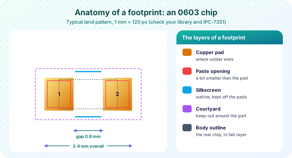
The layers of a footprint
Each footprint spreads across several layers.
- Copper pads carry the electrical connection. Each has a number (or name) that matches a symbol pin. This is the heart of the footprint.
- Solder mask openings expose the pads. They are usually slightly larger than the copper, by about 0.05 mm per side, to allow for alignment errors. The tool often generates them from a rule.
- Paste openings define where the stencil lets solder paste through. For most pads they equal the copper; for large thermal pads they are broken into smaller windows so the paste does not float the part.
- Silkscreen outline shows the body and orientation marks (a dot or line at pin 1). Keep silkscreen off the pads; ink on a pad ruins soldering.
- Courtyard is a thin rectangle that marks the space the part needs, including a margin for assembly. Typical margin: 0.25 mm for small parts (IPC calls levels of 0.1, 0.25 and 0.5 mm). DRC can warn when courtyards overlap.
- Fabrication/assembly layer holds the true body outline and reference text for assembly drawings.
How a land pattern is sized
A solder joint needs copper around the terminal so that solder can climb the side and form a fillet. The standard that governs this is IPC-7351 (and its tools), which defines three density levels: A (most), B (nominal) and C (least). For hand-soldering, bigger pads are friendlier; for dense reflow boards, smaller pads leave room.
For a chip part the pad has three extra dimensions around the terminal: a toe (beyond the outer edge of the terminal), a heel (inside the terminal) and sides. A simple hand-solder-friendly goal is a 0.4 mm toe, 0.1 mm heel and 0.05 mm on each side. Applying it to an 0603 resistor (body 1.6 × 0.8 mm, terminals 0.3 mm long) gives a pad length of 0.3 + 0.4 + 0.1 = 0.8 mm and a pad width of 0.8 + 0.1 = 0.9 mm. The pad centres are 1.6 mm apart (gap between pads 0.8 mm), and the overall footprint is 2.4 mm long. These are typical, not official numbers: libraries that target reflow use smaller toes, and you should follow your library's values or IPC's calculator.
For ICs, the same idea applies, but the main numbers come from the datasheet's recommended land pattern. Many datasheets include a page called "recommended footprint" or "land pattern"; when present, use it, because the manufacturer tested it.
Pin numbering and polarity
Chip resistors and capacitors have no polarity, but pad 1 is still marked. Diodes, LEDs, electrolytic capacitors and every IC have a direction. Common conventions:
- ICs: pin 1 is marked with a dot or notch on the body. Pins number counter-clockwise when viewed from the top, starting at pin 1.
- Diodes and LEDs: pad 1 is usually the cathode in KiCad libraries (mark it on the silkscreen), but conventions differ, so check.
- Polarised capacitors: mark the positive terminal with a plus sign.
A classic fault: viewing from the bottom of the part (as in some datasheets for BGAs and QFNs) while the footprint assumes the top view. Datasheets say "top view" or "bottom view"; read this label.
Verifying a footprint
Footprint mistakes are cheap to catch before ordering. Use this checklist:
- Compare pad count, pitch and pad positions with the datasheet drawing.
- Check the pin numbering against the symbol pinout, pin by pin.
- Print the layout at 1:1 on paper and hold the real part on it. It is the most reliable test, and takes two minutes.
- Check the 3D model if there is one; a misplaced model often reveals a wrong footprint.
- Confirm the exposed pad (if any) is connected to the right net and has a paste layout.
- Make sure the silkscreen does not cover a pad.
Common misconceptions
"Library footprints are always correct." They are written by people. Check every new footprint against the datasheet.
"The courtyard is optional decoration." It protects against parts overlapping and being impossible to place; DRC uses it.
"Pads should be exactly as big as the terminals." Pads need extra copper for the solder fillet. Too small a pad gives weak joints.
Try it
The first example is a land-pattern calculator. It applies the simple toe, heel and side rule from this lesson to four chip sizes. It is a teaching tool, not an IPC calculator, so compare results with your library.
Press Run (or Ctrl + Enter) to see the result here.
Program input · what you'd type while the program runs
Type the answers before you press Run, one per line. Each time the program reads a line (with input()), it gets the next line from this box.
The second example draws the footprint with sliders for toe, heel and side. Watch how the gap between the pads shrinks as the heel grows, and see why a tiny gap is a risk.
Check your understanding
Quick check · 5 questions
of 5 answered You scored / 5 · perfect!
-
1. What is the courtyard used for?
DRC can warn when courtyards overlap. -
2. Why is a pad larger than the terminal it holds?
Toe, heel and side extensions make strong, inspectable joints. -
3. Which is the most reliable footprint check?
A paper test catches pitch and orientation errors fast. -
4. Silkscreen over a pad causes
Keep silkscreen away from pads. -
5. What should you check about a datasheet's footprint drawing orientation?
A bottom view mirrored from the top view leads to reversed pin numbers if misread.
Summary
- A footprint has pads, mask openings, paste openings, silkscreen and a courtyard.
- Pads extend beyond the terminal (toe, heel, sides) so solder fillets form.
- Use the datasheet's recommended land pattern when it exists, and mark pin 1 and polarity.
- Verify by checking against the datasheet and printing at 1:1.
Track your progress
Create a free account to tick off lessons and pick up where you left off on any device.
of PCB Design and Prototyping lessons completed