


















Lesson 39 of 45 · Complete Projects
Project: a 12 V to 3.3 V buck regulator board
Design a 2 A buck regulator board: choose the inductor and capacitors, set the feedback divider, shrink the hot loop, plan thermal vias and check your layout.
A buck converter looks simple on a schematic: an inductor, a capacitor, two switches. On a board it is one of the least forgiving circuits you will lay out, because it carries pulsed current of several amperes with edges of a few nanoseconds. The same schematic can run quietly at 92 % efficiency or radiate, ring and overheat, depending entirely on layout.
This project designs a 12 V to 3.3 V, 2 A module around a synchronous buck IC with integrated switches running at 500 kHz. You will calculate the key parts, then place them in the right order.
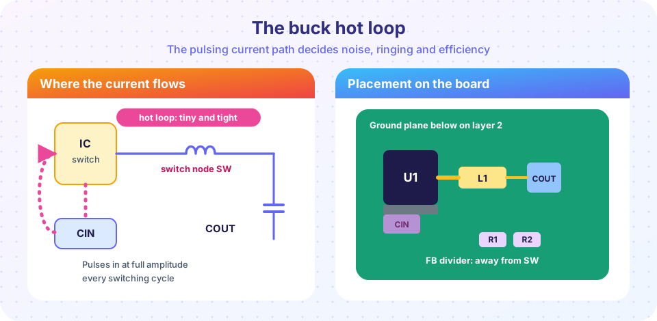
What you will learn
- Compute duty cycle, inductor value, ripple and capacitor requirements.
- Set the output voltage with a feedback divider.
- Identify the hot loop and lay it out first.
- Plan copper, thermal vias and test points for a 2 A rail.
Key terms
Duty cycle (D): the fraction of each period the high-side switch is on; for a buck, D ≈ Vout/Vin.
Hot loop: the loop of input capacitor, high-side switch, low-side switch and ground, carrying pulsed current.
Switch node (SW): the node between the switches and the inductor; it swings from 0 V to Vin each cycle.
Ripple current: the peak-to-peak variation of inductor current, ΔIL.
Feedback (FB) divider: two resistors that scale the output to the regulator's reference voltage.
Requirements and first numbers
Vin = 12 V, Vout = 3.3 V, Iout = 2 A, fsw = 500 kHz.
- Duty cycle:
D = 3.3 / 12 = 0.275. - Inductor: choose ripple of about 30 % of Iout,
ΔIL = 0.6 A. ThenL = (Vin − Vout)·D / (ΔIL·fsw) = 8.7·0.275 / (0.6 · 500 000) ≈ 8.0 µH. Use the next standard value, 8.2 µH, givingΔIL ≈ 0.58 Aand a peak current ofIout + ΔIL/2 ≈ 2.3 A. Choose an inductor whose saturation current is well above that (3 A or more) and whose DC resistance is a few tens of milliohms. - Output capacitor: ripple
ΔVo ≈ ΔIL / (8·fsw·Cout) + ΔIL·ESR. With two 22 µF ceramics, the effective capacitance at 3.3 V DC bias is much lower than the label (often half or less), say 20 µF. ThenΔVo ≈ 0.58 / (8 · 500 000 · 20 µ) ≈ 7 mVplus a small ESR term. - Input capacitor: RMS ripple current
Icin ≈ Iout·√(D·(1−D)) = 2·√(0.275·0.725) ≈ 0.89 A. Ceramic capacitors handle this easily; use at least 10 µF with a voltage rating well above 12 V, bearing in mind the same derating with bias. - Feedback divider: with a 0.8 V reference,
Vout = 0.8·(1 + R1/R2). With R2 = 10 kΩ, R1 = 31.25 kΩ; the nearest E96 value 31.6 kΩ gives 3.33 V. Use 1 % resistors. - Efficiency: assuming 90 %, input power is
3.3·2/0.9 ≈ 7.3 W, so about 0.7 W is dissipated. That heat goes into the IC and the inductor, and the board has to spread it.
Layout, in priority order
- The hot loop first. Place the input capacitor touching the IC's VIN and GND pins, on the same side, with the shortest, widest copper. This loop carries the full pulsed current, and its inductance makes ringing and spikes. Its ring frequency is
f = 1/(2π√(Lloop·Coss)); 5 nH of loop with 200 pF of switch-node capacitance rings near 160 MHz, which is exactly where emission limits are tight. - The switch node small. The SW copper connects the IC to the inductor. Make it just large enough to carry the current. A big SW pour is a transmitting antenna and couples noise into everything.
- Inductor next to SW, then output capacitors close to the inductor, then the load.
- Feedback network away from SW. Route the FB trace from the output after the output capacitors, with the top divider resistor near the output and the bottom resistor near the IC's AGND/FB pin. Keep it short and away from the switch node and the inductor.
- A solid ground plane on layer 2 directly under the loop, so the return current flows beneath the traces; stitch ground with vias near the input and output capacitors.
- Thermal vias under the IC's exposed pad: a grid of 0.3 mm vias on about 1 mm pitch, connecting to the ground plane, so the board spreads the heat.
- Copper for current. At 2 A on 1 oz outside copper and a 10 °C rise, the IPC-2221 width is about 0.8 mm, but use pours: the path is short and wide pours reduce voltage drop.
- Test points: VIN, VOUT, SW (for a scope with a spring ground), PGOOD, and ground near each.
Common misconceptions
"Follow the schematic and it will work." The schematic has no loops. Layout decides emissions and stability.
"Make the switch node plane big for cooling." The inductor and the ground plane cool the IC; a big SW pour only radiates.
"A 22 µF capacitor is 22 µF." Ceramic capacitance falls sharply with DC bias; check the manufacturer's curve.
Try it
Press Run (or Ctrl + Enter) to see the result here.
Program input · what you'd type while the program runs
Type the answers before you press Run, one per line. Each time the program reads a line (with input()), it gets the next line from this box.
Press Run (or Ctrl + Enter) to see the result here.
Program input · what you'd type while the program runs
Type the answers before you press Run, one per line. Each time the program reads a line (with input()), it gets the next line from this box.
Press Run (or Ctrl + Enter) to see the console output here.
No output.
Check your understanding
Quick check · 5 questions
of 5 answered You scored / 5 · perfect!
-
1. What is the duty cycle of an ideal buck from 12 V to 3.3 V?
D = Vout / Vin = 3.3 / 12 = 0.275. -
2. Which loop is the hot loop in a buck converter?
That loop carries pulsed current with fast edges. -
3. Where should the feedback divider go?
Switching noise can corrupt the feedback signal. -
4. Why is the effective capacitance of a ceramic output capacitor often lower than its label?
High-permittivity ceramics lose capacitance under DC bias. -
5. With R2 = 10 kΩ and a 0.8 V reference, which R1 gives about 3.3 V?
R1 = R2 (Vout/Vref − 1) = 10k × 3.125 ≈ 31.3 kΩ; 31.6 kΩ is the closest standard value.
Summary
- Compute D, L, ripple and capacitors from the specification, then choose parts with margin.
- Lay out the hot loop first, keep the switch node small and the feedback node quiet.
- Use a ground plane, thermal vias and pours; add test points.
Next: Chapter 8 review
Track your progress
Create a free account to tick off lessons and pick up where you left off on any device.
of PCB Design and Prototyping lessons completed