


















Lesson 5 of 45 · Getting Started
Chapter 1 Review: Getting Started
Review what a PCB is, how layers and copper weight work and the design workflow, with a recap table and a ten-question quiz covering chapter 1.
You now know what a printed circuit board is, how its layers are built and how a project moves from idea to tested hardware. This review pulls the chapter into one picture, one table and one quiz. If a question surprises you, the lesson it came from is named in the explanation.
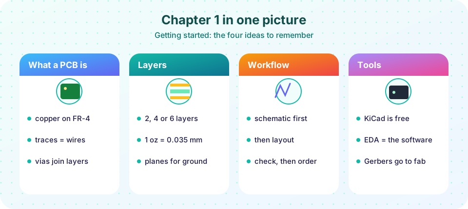
Recap table
| Idea | What to remember |
|---|---|
| Board | Copper on FR-4; traces connect, pads solder, vias join layers |
| Mask and silkscreen | Mask protects copper and keeps solder on pads; silkscreen prints labels |
| Trace resistance | R = ρL/(wt), with ρ = 1.68e-8 Ω·m for copper |
| Copper weight | 1 oz is about 35 µm; sheet resistance about 0.48 mΩ per square |
| Stack-up | Core plus prepreg plus foils; four layers = signal, ground, power, signal |
| Workflow | Requirements, schematic, footprints, layout, checks, build and test |
| Files | Gerbers, drill file, BOM, pick-and-place |
What each lesson covered
- What Is a PCB?: anatomy and the first resistance calculation.
- Layers, Copper Weight and Materials: stack-ups, ounces and why four layers.
- The Design Workflow and Tools: stages, cost of change and manufacturing files.
Check your understanding
Quick check · 10 questions
of 10 answered You scored / 10 · perfect!
-
1. What is the main job of the solder mask?
The mask covers copper except at pads (lesson: What Is a PCB?). -
2. A trace is 50 mm long, 0.25 mm wide, 1 oz copper. Roughly what is its resistance?
R = 1.68e-8 × 0.05 / (0.25e-3 × 35e-6) ≈ 0.096 Ω, about 0.1 Ω. -
3. Which statement about copper weight is correct?
Thickness scales with weight, and resistance per square falls as copper gets thicker. -
4. In a four-layer stack-up, what do the two inner layers usually carry?
Planes give a solid return path and easy power distribution. -
5. What is prepreg?
Prepreg flows and cures in the press, bonding cores and foils. -
6. Which pair is correct?
A via is a plated hole that carries a signal between layers. -
7. What does the dashed loop in the workflow diagram mean?
Design is iterative: checks that fail send you back (lesson: Design Workflow). -
8. Which is NOT a file you send to the factory for the bare board?
Datasheets are for you; the fab needs Gerbers and drill files. -
9. Why choose a four-layer board over two layers for a fast microcontroller design?
A plane next to the signal layer keeps loops small. -
10. Which tool is a free, open-source EDA suite?
KiCad is free and open source.
Summary
- A PCB is a laminated stack of copper and FR-4 with traces, pads, vias, mask and silkscreen.
- Copper weight sets thickness and resistance; stack-ups set how layers are arranged.
- The workflow has six stages and a loop back from failed checks.
Track your progress
Create a free account to tick off lessons and pick up where you left off on any device.
of PCB Design and Prototyping lessons completed