


















Lesson 19 of 45 · Layout and Routing
Trace Width and Current
Calculate PCB trace width for a given current with the IPC-2221 formula, understand temperature rise, internal versus external layers and voltage drop, with runnable examples.
How wide should a trace be? For a signal going into a microcontroller pin, almost any width works because the current is a few microamps. For the 2 A that feeds a motor, a thin trace becomes a heater: it gets hot, its resistance rises, the voltage drops, and in the worst case the copper burns out. The answer depends on current, copper thickness and how much temperature rise you accept.
Fortunately there is a well-known set of curves and a formula that turn this into a calculation, and you can do it in a few lines of code.
What you will learn
- How current heats a trace, and what "10 °C rise" means
- How to use the IPC-2221 formula for external and internal layers
- How to estimate voltage drop and power loss in a trace
- Practical rules for power traces
Key terms
Temperature rise (ΔT): how many degrees the trace becomes hotter than its surroundings.
IPC-2221: the standard that contains the classic trace-current equation (the newer IPC-2152 gives more detailed data).
Mil: one thousandth of an inch, 0.0254 mm; PCB tools often use mils.
Cross-section area (A): trace width times copper thickness.
Voltage drop: the voltage lost along a trace: V = I × R.
Heat in a trace
A current I through a resistance R dissipates power P = I² R. All of that power becomes heat. The trace sheds heat into the board and the air, so it settles at a temperature above its surroundings. Narrower traces have higher resistance (R = ρ L / (w t)) and less surface to shed heat, so they run hotter.
You decide how much rise to accept. A common design value is 10 °C for normal products. In hot environments, or for reliability, use less. Boards can survive much more briefly, but 20 to 30 °C is already hot to the touch and ages the laminate.
The IPC-2221 formula
From measured curves, IPC-2221 gives the following relation between current and cross-section area:
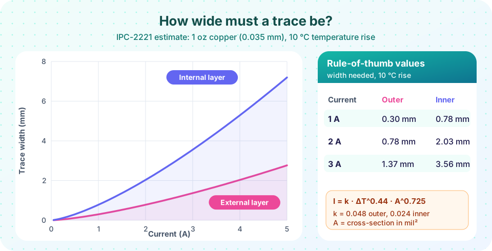
I = k × ΔT^0.44 × A^0.725
Here I is the current in amperes, ΔT the temperature rise in °C, and A the cross-section in square mils (width in mils times thickness in mils). The constant k is 0.048 for external layers and 0.024 for internal layers. Rearranged for area: A = (I / (k × ΔT^0.44))^(1/0.725), and the width is A / thickness.
Thickness for 1 oz copper is 1.378 mil (35 µm). Using the formula for a 10 °C rise, you get, for example, about 0.30 mm for 1 A and 0.78 mm for 2 A on an outer layer. An inner layer needs about 2.6 times the width, because it cannot lose heat to the air: 0.78 mm for 1 A and 2.0 mm for 2 A.
Some observations:
- Width rises faster than current: the exponent 0.725 makes area grow about
I^1.38. Doubling the current needs about 2.6 times the width. - Doubling copper weight to 2 oz roughly halves the required width.
- IPC-2152, the newer standard, shows that a plane close to the trace helps cooling a lot and the internal-layer penalty is smaller than IPC-2221 suggests. IPC-2221 is therefore conservative. It is good for a first design; for products that run near the limit, use IPC-2152 data or measure.
Voltage drop and loss
Temperature is not the only limit. Even a cool trace wastes voltage. For a 50 mm long, 0.3 mm wide trace on 1 oz copper, the resistance is R = 1.68e-8 × 0.05 / (0.3e-3 × 35e-6) = 0.08 Ω. At 1 A the drop is 80 mV, which is 2.4 % of a 3.3 V rail, and the power loss is 80 mW. Such a drop might be acceptable on a logic supply but not for a sensitive analog reference.
For rails, aim for a voltage drop below 1 to 2 % of the supply. If you need lower, widen the trace, shorten it or use a plane.
Practical rules
- Signals: 0.15 to 0.25 mm is typical. Nothing needs more.
- Low power rails (up to 0.5 A): 0.5 mm works.
- 1 A or more: use the calculator, then round up. Consider copper pours instead of traces.
- High current: use a plane or a wide pour, add vias in parallel (several, not one), and leave copper exposed or add thick copper if needed.
- Narrow necks: a trace is only as good as its narrowest part. Where a wide trace must pass between two pads, keep the neck short.
- Pad connections: connect wide traces to the middle of pads, not corners. Use thermal reliefs only where hand soldering needs them.
- Fuses and protection: a trace is not a fuse. Use a real one when a fault could cause a fire.
Common misconceptions
"Wider is always better." Wide traces help current but eat space, add capacitance and can cause solder wicking at pads. Use the width you need, with margin.
"Inner layers carry the same current as outer layers." The IPC-2221 formula says inner layers need about 2.6 times more width for the same rise because they cannot cool into the air.
"The calculator is exact." It is an estimate from tests of simple traces. Real boards depend on neighbouring copper, airflow and enclosures.
Try it
The first example is an IPC-2221 width calculator. Change the current, temperature rise and copper weight to see how the numbers move. The values printed here are from the formula, not from a measurement.
Press Run (or Ctrl + Enter) to see the result here.
Program input · what you'd type while the program runs
Type the answers before you press Run, one per line. Each time the program reads a line (with input()), it gets the next line from this box.
The second example computes resistance, voltage drop and power loss for a trace you describe, then shows how the drop compares with a 1 % budget.
Press Run (or Ctrl + Enter) to see the result here.
Program input · what you'd type while the program runs
Type the answers before you press Run, one per line. Each time the program reads a line (with input()), it gets the next line from this box.
Check your understanding
Quick check · 5 questions
of 5 answered You scored / 5 · perfect!
-
1. On the same 1 oz copper, which trace width carries 1 A for a 10 °C rise (IPC-2221)?
The formula gives about 0.30 mm outside and 0.78 mm inside. -
2. Why do inner layers need wider traces for the same temperature rise?
Heat leaves an outer trace into the air; an inner one is buried in laminate. -
3. How does doubling the copper weight affect the required width?
Area is what carries the current; double thickness halves the width needed. -
4. A 100 mm, 0.5 mm wide, 1 oz trace carries 2 A. About what is its resistance?
R = 1.68e-8 × 0.1 / (0.5e-3 × 35e-6) ≈ 0.096 Ω. -
5. What is the IPC-2221 equation in effect?
It is fitted to test data and is conservative for many boards.
Summary
- Current heats a trace by
I²R; width, copper weight and layer position decide the rise. - IPC-2221:
I = k·ΔT^0.44·A^0.725with k = 0.048 (outer) or 0.024 (inner). - 1 A needs about 0.3 mm outside and 0.78 mm inside for 10 °C on 1 oz copper.
- Check voltage drop too, and prefer planes or pours for high current.
Next: Vias and Layer Changes
Track your progress
Create a free account to tick off lessons and pick up where you left off on any device.
of PCB Design and Prototyping lessons completed