


















Lesson 24 of 45 · Signal and Power Integrity
Impedance and reflections
Learn what characteristic impedance means on a PCB, how trace width and stackup set it, why mismatches cause ringing, and how series termination fixes it, with calculators.
At low frequencies a trace is just a wire: put a voltage at one end and, an instant later, the same voltage appears at the other. At high frequencies that picture breaks. A signal edge takes real time to travel along the copper, and while it travels, the trace behaves like a transmission line: a structure with a definite impedance that the edge "sees" at every point.
If the impedance stays constant from the driver to the receiver, the edge travels cleanly. Wherever it changes (a wider trace, a stub, a connector, the high-impedance input of a chip) part of the edge bounces back, and you see overshoot, undershoot and ringing. Understanding this takes two ideas: characteristic impedance and the reflection coefficient.
What you will learn
- Define characteristic impedance and compute it for a microstrip.
- Explain how width, dielectric height and permittivity change Z0.
- Compute a reflection coefficient and predict ringing.
- Decide when a trace needs termination and choose a series resistor.
Key terms
Characteristic impedance (Z0): the voltage-to-current ratio of a single wave on a line; Z0 = √(L′/C′) for inductance and capacitance per unit length.
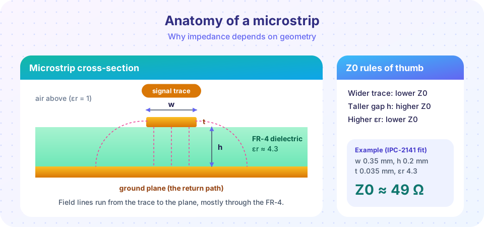
Microstrip: a trace on an outer layer with a plane below it and air above.
Stripline: a trace on an inner layer between two planes.
Reflection coefficient (Γ): the fraction of an incident wave that reflects, Γ = (ZL − Z0)/(ZL + Z0).
Termination: a resistor (or network) that absorbs or damps the wave to stop reflections.
Where Z0 comes from
Cut a tiny slice of trace and ground plane. It has a little series inductance L′ (the loop made by the trace and its return) and a little capacitance C′ to the plane. Chain thousands of these slices together and you get a line whose input looks like a fixed resistor of value Z0 = √(L′/C′), no matter how long the line is. That resistor is not a real dissipating component: it is the ratio of voltage to current the wave carries as it moves.
Three consequences follow directly:
- A wider trace has more capacitance to the plane (and slightly less inductance), so
Z0goes down. - A taller dielectric between trace and plane (bigger
h) has less capacitance and more loop inductance, soZ0goes up. - A higher permittivity
εrraises capacitance and lowersZ0. It also slows the wave.
For a surface microstrip, the classic IPC-2141 approximation is
Z0 ≈ 87 / √(εr + 1.41) · ln( 5.98·h / (0.8·w + t) )
with w the trace width, h the dielectric height, t the copper thickness and εr the relative permittivity of the board. It is valid roughly for 0.1 < w/h < 2.0. Field solvers (and your board house's impedance calculator) are more accurate, but this formula is good for a first estimate and for building intuition.
Take FR-4 with εr ≈ 4.3, h = 0.2 mm, t = 0.035 mm (1 oz copper) and a trace w = 0.35 mm wide. The formula gives about 49 Ω, very close to the 50 Ω that single-ended RF and many digital standards use.
Why 50 Ω, and why 90 or 100 Ω for pairs
Fifty ohms is a historical compromise between low loss and power handling in coaxial cable. On boards it stuck because it is easy to reach with common stackups. Differential pairs are specified by the impedance between the two lines: 90 Ω for USB 2.0, 100 Ω for Ethernet and many LVDS buses. These values are set by the standards, so the stackup and spacing must be designed to hit them, usually with the fab's calculator.
How a reflection happens
A wave travelling on a line of impedance Z0 arrives at a load ZL. The load must obey Ohm's law: the total voltage across it divided by the total current through it equals ZL. The incident wave alone does not satisfy that unless ZL = Z0, so a reflected wave appears to fix the difference. Its size relative to the incident wave is
Γ = (ZL − Z0) / (ZL + Z0)
| Load | Γ | What happens |
|---|---|---|
ZL = Z0 |
0 | Everything absorbed, no reflection. |
Open (ZL → ∞) |
+1 | Full reflection, same polarity: the voltage at the end doubles. |
Short (ZL = 0) |
−1 | Full reflection, inverted: voltage at the end is zero. |
ZL = 100 Ω, Z0 = 50 Ω |
+1/3 | A third of the wave comes back. |
A CMOS input is almost an open circuit at low frequency, so the receiving end reflects with Γ ≈ +1. If the driver's output resistance is much lower than Z0, the reflection arriving back at the driver bounces again, with the opposite sign (Γs negative). The edge ping-pongs along the line and settles after several round trips: that is ringing.
Series termination
The simplest fix for a point-to-point digital line is to add a series resistor near the driver so that driver resistance plus resistor equals Z0:
Rseries = Z0 − Rdriver
The line now sees a source that matches it, so the reflection from the open receiver is absorbed when it returns. The receiver gets a clean full-swing edge after one round trip. Typical values are 22 Ω to 33 Ω for drivers with 17 to 27 Ω output resistance on 50 Ω lines. The trade-off is that the edge reaches the middle of the line at half amplitude, so series termination only suits point-to-point connections, not buses with several receivers along the way.
How long is "long"?
Reflections only matter when the edge is still changing while the reflection returns. A widely used rule says: treat the trace as a transmission line when its one-way delay exceeds about one sixth to one quarter of the signal rise time. On FR-4 a surface trace delays a signal by about 6 ns per meter (roughly 150 ps per inch), and an inner stripline by about 7 ns per meter. So a 1 ns edge makes a trace "long" at around 2.5 to 3 cm, while a 10 ns edge allows more than 25 cm. That is why a slow I²C bus ignores all of this and a USB or SPI-at-50-MHz bus cannot.
Common misconceptions
"Z0 is a resistor I can measure with a multimeter." It is not. Z0 is a property of the trace geometry that governs a travelling wave; a meter on a 50 Ω line reads the DC resistance of the copper, a few milliohms.
"Controlled impedance is only for RF." Any fast digital net on a long trace benefits from controlled impedance. Ask your board house to build to a stackup you specify.
"Ringing is just noise." It is deterministic. It can be predicted from Γ and the line delay, and removed by changing the circuit.
Try it
Press Run (or Ctrl + Enter) to see the result here.
Program input · what you'd type while the program runs
Type the answers before you press Run, one per line. Each time the program reads a line (with input()), it gets the next line from this box.
The next demo follows an edge as it bounces. It is a calculator of the reflection formulas above, not a full circuit simulator.
Press Run (or Ctrl + Enter) to see the result here.
Program input · what you'd type while the program runs
Type the answers before you press Run, one per line. Each time the program reads a line (with input()), it gets the next line from this box.
Finally, a quick calculator for the "how long is long" rule.
Press Run (or Ctrl + Enter) to see the console output here.
No output.
Check your understanding
Quick check · 5 questions
of 5 answered You scored / 5 · perfect!
-
1. Which change lowers the characteristic impedance of a microstrip?
A wider trace has more capacitance to the plane, so Z0 drops. A thicker dielectric or lower permittivity raises it. -
2. A 50 ohm line drives a 100 ohm load. What is the reflection coefficient?
Γ = (100 − 50) / (100 + 50) = 50/150 = 1/3. -
3. A driver has 20 ohm output resistance and the line is 50 ohm. What series resistor matches the source?
Rseries = Z0 − Rdriver = 50 − 20 = 30 ohm. -
4. Why does series termination not work well for a bus with several receivers along the line?
With a source-matched design the incident wave is half amplitude, and the full voltage appears only after the reflection from the far end returns. -
5. A trace is about 6 ns per meter. For a 1 ns edge and the one-sixth rule, about how long is the critical length?
Critical flight time is 1 ns / 6 = 0.167 ns. At 6 ns/m that is 0.167/6 m = 0.028 m, or 2.8 cm.
Summary
- A trace is a transmission line with impedance
Z0set by its width, dielectric height, copper thickness andεr. - The IPC-2141 formula gives a first estimate of microstrip
Z0; the fab's field solver gives the final answer. - A mismatch reflects part of the wave:
Γ = (ZL − Z0)/(ZL + Z0). - A series resistor of
Z0 − Rdrivernear the driver tames point-to-point lines. - Treat a trace as a transmission line when its delay exceeds about one sixth of the rise time.
Track your progress
Create a free account to tick off lessons and pick up where you left off on any device.
of PCB Design and Prototyping lessons completed