


















Lesson 11 of 45 · Components and Footprints
Chapter 3 Overview: Components and Footprints
Overview of chapter 3: passive values and tolerances, package families, footprints and land patterns, and how to read a datasheet before choosing a part.
A schematic symbol is an idea; a footprint is the real thing. It is the pattern of copper pads on which a physical component will be soldered. If the footprint does not match the package, the part will not fit, and no amount of clever layout will rescue the board. This is why many experienced designers spend more time on the parts and footprints than on routing.
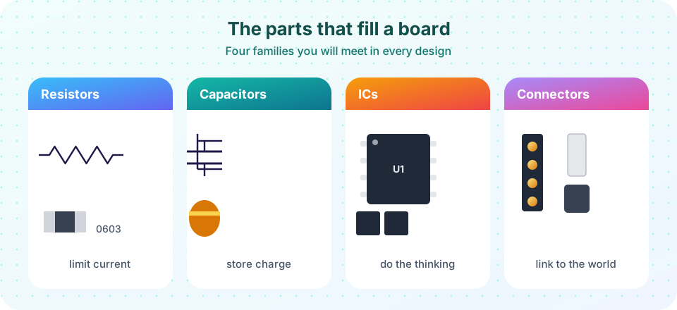
This chapter covers the components that fill almost every board, the packages they come in, how to design or check a footprint and how to read the datasheet that tells you everything you need to know.
From symbol to solder
Passives
Packages
Footprints
Datasheets
What you will learn in this chapter
- Standard values, tolerances and ratings of resistors and capacitors
- The names and sizes of chip and IC packages, and when to use which
- How a footprint is built from pads, silkscreen and a courtyard
- How to read a datasheet and choose between similar parts
The lessons
- Passives and Preferred Values: E-series, tolerance, voltage rating and dielectric types.
- Packages: SMD and Through-Hole: chip sizes, IC packages and how to choose.
- Footprints and Land Patterns: what is in a footprint and how to make a reliable one.
- Choosing Parts and Reading Datasheets: ratings, derating and sourcing.
- Chapter 3 Review: recap and quiz.
Why this chapter matters
Most "my board does not work" stories start with a part problem: a footprint that was drawn from memory, a capacitor whose capacitance collapses under bias voltage, a regulator that overheats because nobody read the thermal figures. These are cheap to prevent. The habit to build is simple: before you place any part, find its datasheet and read three pages: ratings, pinout and package drawing.
You will also learn to use libraries. Your EDA tool ships thousands of footprints, and the manufacturer often supplies one too. Libraries save time, but they contain mistakes, so you verify them. The next lessons show how.
Check your understanding
Quick check · 3 questions
of 3 answered You scored / 3 · perfect!
-
1. What is a footprint?
A footprint is the land pattern that matches the real package. -
2. Which pair is the symbol-to-footprint relationship?
Symbols belong to the schematic; footprints to the layout. -
3. What should you read before placing a new part?
Ratings, pinout and package drawing prevent most part errors.
Summary
- A footprint is the pad pattern that matches a real package.
- This chapter covers passives, packages, footprints and datasheets.
- Verify every footprint and read every datasheet before ordering.
Track your progress
Create a free account to tick off lessons and pick up where you left off on any device.
of PCB Design and Prototyping lessons completed