


















Lesson 4 of 45 · Getting Started
The Design Workflow and Tools
Follow the six stages of PCB design from requirements to testing, meet the common EDA tools such as KiCad and learn what files you send to the factory.
Professionals do not start by drawing traces. They start by writing down what the board must do, and they finish by testing it. In between sits a sequence of steps, each of which produces files that the next step uses. If you follow the sequence, mistakes are caught early, when they are cheap to fix. If you skip steps, you pay for it with a board that does not work.
This lesson describes the stages, introduces the tools and shows what a board "looks like" as a set of files.
What you will learn
- The six stages of a PCB project and what each produces
- Why mistakes get more expensive at each stage
- The main EDA tools and how KiCad is organised
- Which files the factory needs
Key terms
Requirements: the list of what the board must do (voltages, interfaces, size, cost).
DRC (design rule check): software that checks the layout against the factory's limits.
Gerber files: the standard files, one per layer, that describe copper, mask and silkscreen to the factory.
Drill file: a list of hole positions and diameters (often Excellon format).
Pick-and-place file: part positions and rotations used by assembly machines.
The six stages
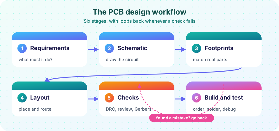
- Requirements. Write down inputs, outputs, supply voltage, maximum current, size, cost and where it will be used (indoors, a car, a wet place). "A board that reads a temperature sensor and sends it over USB" is a start; "3.3 V logic, USB-C, 30 × 20 mm, below 5 USD per board" is a specification.
- Schematic. Draw the circuit with symbols. Run the electrical rules check. The output is a netlist.
- Footprints. Give each symbol a footprint, the pad pattern of the real part. Wrong footprints are one of the most common beginner mistakes, so this stage deserves care.
- Layout. Set the board outline and rules, place parts, route traces, add planes and silkscreen.
- Checks. Run DRC, review the board visually and in 3D, compare against the schematic, generate Gerbers and look at them in a separate viewer.
- Build and test. Order the board, assemble it, power it carefully, test and debug.
The dashed loop in the picture matters. If testing shows a mistake, you change the design and order again. Professionals plan for this: a first prototype is expected to have one or two issues.
Why early checks pay off
A rule of thumb in engineering says that the cost of fixing a defect rises by about an order of magnitude with each stage it survives. The numbers are illustrative, but the pattern is real. Changing a resistor value on the schematic takes a minute. Moving a trace takes an hour. Discovering a wrong footprint after the boards arrive means a new order, a week of waiting and money. Discovering it after thousands of units have shipped is a recall.
This is why every stage ends with a check, and why you read your own schematic aloud, pin by pin, before you start layout.
The tools
All PCB tools do the same jobs: schematic capture, layout, library management, checks and file export. They differ in price, learning curve and ecosystem.
| Tool | Notes |
|---|---|
| KiCad | Free and open source, runs on Windows, macOS and Linux, widely used in industry and education. |
| Altium Designer | Professional paid suite, very common in companies. |
| Autodesk Eagle / Fusion | Popular with hobbyists in the past; now part of Fusion. |
| EasyEDA | Browser-based, connected to a fabrication and parts service. |
| Others | OrCAD, Cadence Allegro, Zuken and Horizon EDA for large companies or special needs. |
This course uses KiCad terms as examples (Eeschema/Schematic Editor, PCB Editor, Footprint Editor), but concepts transfer. A KiCad project is a folder with a handful of files: a .kicad_pro project, a .kicad_sch schematic and a .kicad_pcb board. It is a good habit to keep that folder in version control, such as Git, so you can undo mistakes and see changes.
What the factory needs
When you finish, you export a package of manufacturing files:
- Gerber files for each copper layer (
.gtltop copper,.gblbottom copper and so on), the solder mask on each side, silkscreen on each side and the board outline. - A drill file for plated and unplated holes.
- For assembly, a bill of materials (BOM) and a pick-and-place (placement) file.
A zip file of these is what you upload to a fab. Chapter 6 covers it in detail. A good habit: open the Gerbers in a free viewer (KiCad includes one) before ordering. You are looking at exactly what the factory will see.
Common misconceptions
"I can fix the schematic later while I route." Changing a schematic after layout is possible but messy. Finish the schematic and review it first.
"The software will warn me about every mistake." ERC and DRC catch rule violations, not design errors. A resistor with the wrong value passes every check.
"Autorouters design the board for me." Autorouters connect wires but do not understand your circuit. They are tools for after you have placed parts well, and they rarely produce good results for power or fast signals.
Try it
The first example models the cost of change. The numbers are an illustrative model, not measured data; the lesson is the shape of the curve.
Press Run (or Ctrl + Enter) to see the console output here.
No output.
The second example is a checklist you can tick off as you read this lesson. It stores nothing; it only shows progress, as a model for a real design-review checklist.
Check your understanding
Quick check · 5 questions
of 5 answered You scored / 5 · perfect!
-
1. Which stage comes immediately after the schematic is checked?
Each symbol needs a footprint before the netlist can create a layout. -
2. What does DRC check?
DRC checks spacing, widths and similar rules, not the logic of the circuit. -
3. Which tool is free and open source?
KiCad is free and open source and widely used. -
4. What are Gerber files?
Gerbers describe copper, mask, silkscreen and outline for each layer. -
5. Why does the cost of a mistake grow at each stage?
A late fix means repeating work, ordering again and waiting.
Summary
- A project runs from requirements through schematic, footprints, layout and checks to build and test.
- Mistakes grow far more expensive the later they are found, so check at every stage.
- KiCad is a free tool; the concepts apply to any EDA suite.
- The factory needs Gerbers, a drill file and, for assembly, a BOM and placement file.
Next: Chapter 1 Review
Track your progress
Create a free account to tick off lessons and pick up where you left off on any device.
of PCB Design and Prototyping lessons completed