


















Lesson 15 of 46 · Crystal Structures and Defects
Crystal Defects: Vacancies, Dislocations and Grain Boundaries
Learn the point, line, planar and volume defects of crystals, calculate vacancy concentration from temperature, and relate grain size to strength with Hall-Petch.
The perfect crystals of the last lessons are idealizations. Real crystals always contain defects, and many of the most useful properties of materials exist because of them. Silicon is a good semiconductor only because we add a few parts per million of impurity atoms. Steel is strong because of defects that block other defects. Atoms can move through a solid, which makes carburizing and annealing possible, only because there are vacant sites. If metals were perfect crystals they would be about a hundred to a thousand times stronger than they are, and also far less useful, because they could not be bent or shaped. So this lesson is a catalog of what is wrong with crystals, and why it is a good thing.
What you will learn
- The four classes of defects by dimension: point, line, planar and volume.
- How vacancy concentration depends on temperature through an Arrhenius law.
- What dislocations are, the meaning of the Burgers vector, and how density is quoted.
- How grain boundaries and grain size (ASTM number) affect strength.
Key terms
Vacancy: an empty lattice site where an atom is missing.
Interstitial: an extra atom squeezed into a space between lattice sites.
Dislocation: a line defect around which atoms are displaced; the boundary of a region that has slipped.
Burgers vector b: the vector that measures the lattice distortion around a dislocation, one lattice spacing in a close-packed direction.
Point defects (0D)
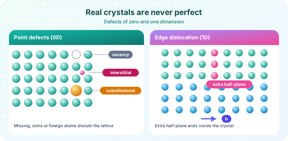
A vacancy is a missing atom. Vacancies exist in every crystal at every temperature above absolute zero, because creating them raises the energy but also raises the entropy (disorder), and the balance favors a small number. The equilibrium fraction of vacant sites is
N_v / N = exp(−Q_v / k_B T)
where Q_v is the energy to form a vacancy (about 0.9 eV for copper) and k_B = 8.617 × 10⁻⁵ eV/K. At 300 K this gives about 10⁻¹⁵ for copper, essentially none. At 1000 K it is about 3 × 10⁻⁵ and at the melting point (1358 K) about 5 × 10⁻⁴: one site in two thousand is empty. Vacancies matter because atoms move by hopping into them, so diffusion rates follow the same exponential law (chapter 6).
A self-interstitial is an extra atom of the host squeezed between normal sites. It costs a great deal of energy (typically several eV) because the surrounding atoms are crowded, so there are far fewer self-interstitials than vacancies. Impurity atoms may be substitutional (replacing a host atom) or interstitial (small atoms in the holes, as for carbon in iron). A solid solution of the second kind is formed when the solute atom is small; the Hume-Rothery rules predict extensive substitutional solid solution when the two atoms differ in size by less than about 15 %, have the same crystal structure, similar electronegativity and the same valence. Copper and nickel meet all four conditions, and they form a solid solution over the whole composition range.
In ionic crystals charge must be balanced, so defects come in pairs. A Schottky defect is a pair of missing ions, one cation and one anion. A Frenkel defect is a vacancy plus an interstitial of the same ion. These defects make ionic conduction possible, and impurity ions with a different charge can create vacancies as well, as in the oxygen-vacancy conductors of fuel cells.
Press Run (or Ctrl + Enter) to see the result here.
Program input · what you'd type while the program runs
Type the answers before you press Run, one per line. Each time the program reads a line (with input()), it gets the next line from this box.
Line defects: dislocations (1D)
A dislocation is a line along which the lattice is distorted. The easiest to picture is the edge dislocation: imagine inserting an extra half-plane of atoms into the crystal, so that it ends part-way in. The edge of that half-plane is the dislocation line. Above it the lattice is compressed, below it stretched. A screw dislocation has the lattice sheared around the line so that planes spiral like a ramp. Real dislocations are usually mixed.
The Burgers vector b is found by drawing a circuit that would close in a perfect crystal. Around a dislocation it fails to close by a vector, which is b. For an edge dislocation b is perpendicular to the line, for a screw it is parallel, and in each case it is a lattice translation. The magnitude is a/√2 for FCC metals (the nearest-neighbor distance, 0.256 nm for copper) and a√3/2 for BCC metals.
Dislocations move under shear stress and carry plastic deformation: a dislocation gliding across a plane shifts the part of the crystal above it by one b (the next lesson explains why this needs far less stress than shearing a whole plane at once). Dislocation density ρ_d is the total length of dislocation line per unit volume, in m⁻² (meters per cubic meter). A well-annealed metal has 10¹⁰ to 10¹² m⁻², a heavily cold-worked one 10¹⁴ to 10¹⁶ m⁻², and a good silicon wafer almost none. Dislocations are seen in transmission electron microscopes as dark lines and as etch pits on a polished surface.
Planar defects (2D)
The most important planar defect is the grain boundary, the interface between two grains with different orientations. Atoms at the boundary do not fit either lattice, so the boundary has extra energy and is a region of faster diffusion. In a low-angle boundary (misorientation under about 15°) the mismatch is accommodated by an array of dislocations; high-angle boundaries are more disordered. A twin boundary is a mirror plane where the lattice on one side is the reflection of the other; twins form during deformation (hexagonal metals) or annealing (copper, brass). A stacking fault is a mistake in the stacking sequence, such as an extra layer in ABCABC. External surfaces are also planar defects, since surface atoms have missing neighbors.
Grain boundaries strengthen metals because dislocations cannot easily cross them. The finer the grains, the more boundaries there are in a dislocation's path. The relationship, found by Hall and by Petch in the early 1950s, is
σ_y = σ₀ + k d^(−1/2)
where d is the average grain diameter and σ₀, k are constants of the material. Grain size is often reported as the ASTM number G, defined by N = 2^(G − 1) grains per square inch in a photomicrograph at 100× magnification. A larger G means smaller grains. That corresponds to about 15.5 × 2^(G − 1) grains per mm² on the real surface, so G = 5 means about 250 grains/mm² and a mean diameter near 60 µm.
Press Run (or Ctrl + Enter) to see the result here.
Program input · what you'd type while the program runs
Type the answers before you press Run, one per line. Each time the program reads a line (with input()), it gets the next line from this box.
Volume defects (3D)
Voids and pores in castings and sintered ceramics, cracks, inclusions of foreign particles and precipitates of a second phase are three-dimensional defects. Some are harmful: a pore or crack concentrates stress and starts fracture (chapter 4). Others are designed in: fine precipitates in aluminum alloys and nickel superalloys block dislocations and strengthen the material (chapter 6).
Seeing defects
Metallographers cut a sample, grind and polish it to a mirror, and then etch it with an acid. Grain boundaries are attacked faster than grain interiors and show up as dark lines under an optical microscope, so grain size can be measured. Transmission electron microscopes reveal dislocations and precipitates, and X-ray topography maps dislocations in semiconductor wafers.
Common misconceptions
"Defects always weaken materials." Vacancies enable diffusion; dislocations enable shaping; grain boundaries and precipitates strengthen. Controlling defects is how engineers control properties.
"A dislocation is a crack." A crack is a free surface; a dislocation is a line of lattice distortion with no gap, and moving dislocations deform a metal without breaking it.
"A larger ASTM grain size number means larger grains." The opposite: G rises as grains get smaller because N doubles with each unit of G.
Check your understanding
Quick check · 5 questions
of 5 answered You scored / 5 · perfect!
-
1. Which defect is a missing atom?
A vacancy is an empty lattice site. -
2. How does the equilibrium vacancy fraction change with temperature?
N_v/N = exp(−Q_v/k_B T) rises rapidly as T increases. -
3. An edge dislocation has a Burgers vector that is
For an edge dislocation b is perpendicular to the line; for a screw it is parallel. -
4. Grain boundaries strengthen a metal because
Dislocations pile up at boundaries; smaller grains mean more obstacles (Hall-Petch). -
5. Which Hume-Rothery condition favors extensive substitutional solid solution?
Similar atom size, structure, electronegativity and valence promote solubility.
Summary
- Defects are classified by dimension: point (vacancy, interstitial, substitutional), line (dislocation), planar (grain boundary, twin, surface) and volume (pores, precipitates, cracks).
- The equilibrium vacancy fraction is
exp(−Q_v/k_B T)and controls diffusion. - Dislocations are lines with a Burgers vector
b; density runs from about 10¹⁰ to 10¹⁶ m⁻². - Grain boundaries block dislocations;
σ_y = σ₀ + k d^(−1/2); ASTM G rises as grains shrink. - Real materials get their useful properties from controlled defects.
Next: Chapter 3 Review
Track your progress
Create a free account to tick off lessons and pick up where you left off on any device.
of Materials Science lessons completed