


















Lesson 21 of 45 · The PN Junction
Chapter 4 Review: The PN Junction
Review chapter 4: built-in voltage, depletion width, the ideal diode equation, junction capacitance and breakdown mechanisms, with a ten-question quiz.
The PN junction is the first real device of the course, and you can now describe it in four situations: at rest, forward biased, reverse biased and broken down. Each one is a variation on the same physics: drift and diffusion of carriers in a depletion region whose width responds to voltage.
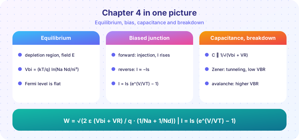
Recap table
| Lesson | Key idea | Formula |
|---|---|---|
| Equilibrium | Depletion region, built-in field | Vbi = (kT/q) ln(Na Nd/ni²); W = √(2εVbi/q · (1/Na + 1/Nd)) |
| I-V characteristics | Minority carrier injection | I = Is (e^(V/VT) − 1); 60 mV per decade |
| Capacitance and breakdown | Stored charge, high-field limits | Cj ∝ (Vbi + VR)^(−1/2); Zener vs avalanche |
Try it
The first example is a one-stop junction calculator: give it a doping and a bias, and it returns the depletion width, capacitance and current.
Press Run (or Ctrl + Enter) to see the result here.
Program input · what you'd type while the program runs
Type the answers before you press Run, one per line. Each time the program reads a line (with input()), it gets the next line from this box.
Press Run (or Ctrl + Enter) to see the console output here.
No output.
Check your understanding
Quick check · 10 questions
of 10 answered You scored / 10 · perfect!
-
1. Vbi of a silicon junction with Na = 10¹⁷ and Nd = 10¹⁶ cm⁻³ is approximately
Vbi = 0.02585 × ln(10³³/10²⁰) ≈ 0.77 V. -
2. In equilibrium, which quantity is flat across the junction on the band diagram?
A flat EF means zero net current; the bands bend instead. -
3. Forward bias makes the depletion region
The barrier falls to Vbi − V, so less depleted charge is needed. -
4. What happens to diode current when forward voltage increases by 120 mV at 300 K?
Each 59.5 mV gives a factor of 10, so 120 mV gives about 100. -
5. Is is proportional to
Is = A q ni² (…), so it rises very rapidly with temperature. -
6. A C-V measurement plots 1/C² against VR. The slope gives
The slope is 2/(q ε N A²) for a one-sided abrupt junction. -
7. Which junction breaks down mainly by tunneling?
Thin depletion regions and very high fields allow band-to-band tunneling. -
8. The temperature coefficient of the avalanche breakdown voltage is
More lattice scattering at high temperature makes ionization harder. -
9. Diffusion capacitance Cd equals
It represents stored minority charge Q = I τ per volt. -
10. In a p⁺n junction the depletion region lies mainly
Na xp = Nd xn: the lightly doped side must give up more width to supply the same charge.
Summary
- Vbi, W and Emax follow from the depletion approximation; the lighter side is wider.
- I = Is (e^(V/VT) − 1): reverse saturation, forward exponential, 60 mV per decade.
- Cj ∝ (Vbi + VR)^(−1/2); diffusion capacitance Cd = τI/VT in forward bias.
- Breakdown by Zener tunneling (low voltage) or avalanche (higher voltage).
- Chapter 5 puts two junctions back to back and turns the diode into an amplifier.
Track your progress
Create a free account to tick off lessons and pick up where you left off on any device.
of Semiconductor Devices lessons completed