


















Lesson 19 of 45 · The PN Junction
Diode Current-Voltage Characteristics: The Ideal Diode Equation
Learn how forward and reverse bias change a PN junction, derive the ideal diode equation I = Is(e^(V/VT) − 1), and solve a diode and resistor circuit.
A diode conducts well in one direction and hardly at all in the other. This is the first behavior you saw in the course map, and now we can explain its origin and compute it. The explanation is a story about minority carriers: forward voltage lowers the barrier, injects carriers across the junction, and those carriers diffuse and recombine on the other side.
The result is the Shockley ideal diode equation, with a saturation current Is that depends on the material and the doping, and an exponential factor that carries the temperature through kT/q.
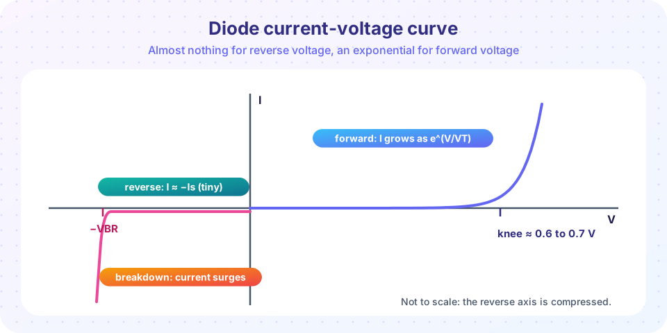
What you will learn
- What forward and reverse bias do to the barrier and the depletion width.
- How the minority-carrier injection leads to I = Is (e^(V/VT) − 1).
- How Is depends on doping, diffusion length and temperature.
- How to solve for the operating point of a diode with a series resistor, and when real diodes deviate.
Key terms
- Forward bias: p side positive relative to n side; the barrier shrinks to Vbi − V.
- Reverse bias: p side negative; the barrier grows to Vbi + VR.
- Saturation current Is: the tiny reverse current of the ideal diode, set by minority carriers.
- Ideality factor n: a number between 1 and 2 in I = Is (e^(V/(n VT)) − 1) accounting for recombination in the depletion region.
Biasing the junction
Forward bias applies a voltage V with the p side positive. The applied voltage opposes the built-in field, so the total barrier falls from Vbi to Vbi − V and the depletion region narrows. More carriers can diffuse across: electrons from n to p, holes from p to n.
Reverse bias applies VR with the p side negative. The barrier grows to Vbi + VR, the depletion region widens, and almost no majority carriers cross.
The law of the junction
In equilibrium the electron density on the p side at the depletion edge is the minority density np0 = ni²/Na. With bias V, the barrier changes by qV, and Boltzmann statistics gives
np(−xp) = np0 · exp(V / VT)        (VT = kT/q)
pn(xn)  = pn0 · exp(V / VT)
At V = 0.6 V and 300 K, exp(0.6/0.02585) ≈ 1.2 × 10¹⁰: the minority density at the edge is 10 billion times its equilibrium value. Those injected carriers form an excess that diffuses away from the junction and recombines. Far from the junction, the excess falls to zero:
Δnp(x) = np0 (e^(V/VT) − 1) · exp(−(x + xp)/Ln) (in the p region, x < −xp)
where Ln = √(Dn τn) is the diffusion length.
The ideal diode equation
The diffusion current at the depletion edge is Dn times the gradient of the excess density. Adding electron and hole contributions gives the total current:
I = Is (e^(V/VT) − 1)

Is = A q ni² ( Dn / (Ln Na) + Dp / (Lp Nd) )
Look at the structure of Is. It is proportional to ni², so it rises steeply with temperature (about 15 percent per kelvin near 300 K in silicon, doubling in about 4.5 K). It falls with more doping, because heavily doped sides have few minority carriers. And it scales with the junction area A.
For V negative by several VT, the exponential vanishes and I → −Is: a constant reverse saturation current, tiny (10⁻¹⁵ to 10⁻¹² A for small silicon diodes). For V positive by a few VT, I ≈ Is e^(V/VT): each 59.5 mV increase multiplies the current by 10.
Worked example
A silicon junction with area A = 10⁻⁴ cm² (100 µm × 100 µm), Na = 10¹⁷, Nd = 10¹⁶ cm⁻³, Dn = 25 cm²/s, Dp = 10 cm²/s, and lifetimes τ = 1 µs on both sides (Ln = 50 µm, Lp = 32 µm):
A q ni² = 1e-4 × 1.602e-19 × 1e20 = 1.6e-3
Dn/(Ln Na) = 25 / (5e-3 × 1e17)  = 5.0e-14
Dp/(Lp Nd) = 10 / (3.16e-3 × 1e16) = 3.2e-13
Is = 1.6e-3 × 3.7e-13 ≈ 5.9e-16 A
For a forward current of 1 mA: V = VT ln(I/Is) = 0.02585 × ln(1.7 × 10¹²) = 0.02585 × 28.2 ≈ 0.73 V. That is why silicon diodes are said to "drop about 0.7 V". The number is not a property of the diode alone; it is the voltage needed for the current of interest.
Real diodes and temperature
At small forward currents, recombination inside the depletion region adds a component that goes as e^(V/(2VT)), so the ideality factor n approaches 2. At very high currents, series resistance and high-level injection cause the curve to bend toward a straight line. In reverse bias, the thermal generation of carriers inside the widening depletion region adds a generation current that grows slowly with reverse voltage and usually exceeds Is in silicon at room temperature.
At a fixed current, the forward voltage falls with temperature by roughly 1.5 to 2 mV per kelvin because Is rises faster than VT. That is exactly how diode-connected transistors are used as temperature sensors.
Try it
The first example plots the diode equation for three temperatures on a log scale and shows how the forward voltage at constant current falls as the device warms.
Press Run (or Ctrl + Enter) to see the result here.
Program input · what you'd type while the program runs
Type the answers before you press Run, one per line. Each time the program reads a line (with input()), it gets the next line from this box.
Press Run (or Ctrl + Enter) to see the result here.
Program input · what you'd type while the program runs
Type the answers before you press Run, one per line. Each time the program reads a line (with input()), it gets the next line from this box.
Common misconceptions
"A silicon diode always drops exactly 0.7 V." The voltage depends on the current: it changes by about 60 mV per decade. 0.7 V is a convenient approximation for currents of milliamps.
"Reverse current is zero." It is small, but not zero, and it rises sharply with temperature, doubling about every 5 to 10 K.
Check your understanding
Quick check · 5 questions
of 5 answered You scored / 5 · perfect!
-
1. Under forward bias V, the minority electron density at the p-side depletion edge is multiplied by
The law of the junction gives np(−xp) = np0 exp(V/VT). -
2. For V much less than −VT, the diode current approaches
The exponential vanishes, leaving I = −Is. -
3. A forward voltage increase of 59.5 mV at 300 K multiplies the current by
exp(59.5 mV / 25.85 mV) = exp(2.303) = 10. -
4. A diode has Is = 10⁻¹⁵ A. What forward voltage gives 1 mA at 300 K?
V = VT ln(I/Is) = 0.02585 × ln(10¹²) = 0.02585 × 27.6 ≈ 0.71 V. -
5. Why does the forward voltage at constant current fall as temperature rises?
Is ∝ ni² grows very fast with T, so less voltage is needed for the same current.
Summary
- Forward bias lowers the barrier to Vbi − V and injects minority carriers; reverse bias raises it.
- Law of the junction: np(−xp) = np0 e^(V/VT).
- I = Is (e^(V/VT) − 1), Is = A q ni² (Dn/(Ln Na) + Dp/(Lp Nd)).
- Forward voltage depends logarithmically on current and falls roughly 1.5 to 2 mV/K.
- Real diodes show ideality factors up to 2, series resistance and generation current.
Track your progress
Create a free account to tick off lessons and pick up where you left off on any device.
of Semiconductor Devices lessons completed