


















Lesson 43 of 45 · Projects and Practice
Glossary of semiconductor devices
A searchable glossary of more than 80 semiconductor device terms covering bands, carriers, junctions, BJTs, MOSFETs, optoelectronics and fabrication, with flash cards for review.
Semiconductor physics has a large vocabulary, and many words sound alike (V_T the thermal voltage versus V_T the threshold voltage; recombination versus generation; base versus body). This glossary collects the terms of the whole course in one place, grouped by topic, with a live search and a flash-card review below the tables.
What you will learn
- A precise one-line meaning for the most important terms in the field.
- Which symbols are overloaded and how to tell them apart from context.
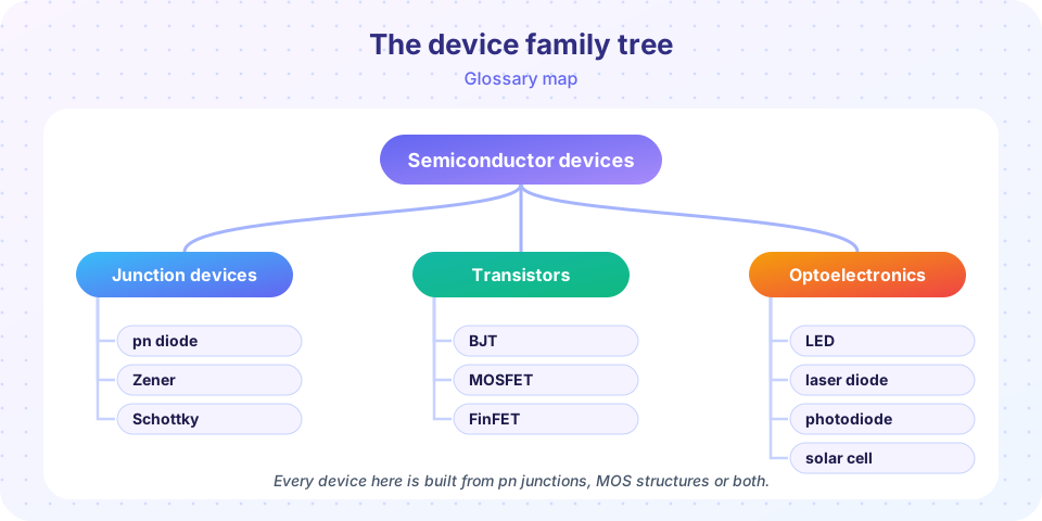
- How the terms group into families so you can recall them as a map.
Bands, carriers and doping
| Term | Meaning |
|---|---|
| Band gap (E_g) | Energy separating the top of the valence band from the bottom of the conduction band; 1.12 eV for silicon. |
| Conduction band | Band of allowed energies in which electrons are free to carry current. |
| Valence band | Highest filled band at absolute zero; missing electrons here behave as holes. |
| Direct band gap | Gap in which band extrema share the same crystal momentum, so light is emitted efficiently (GaAs, GaN). |
| Indirect band gap | Gap that needs a phonon for a transition (Si, Ge); poor light emitters. |
| Electron | Negative mobile charge carrier in the conduction band. |
| Hole | Positive mobile carrier representing a missing electron in the valence band. |
| Intrinsic semiconductor | Pure material with n = p = n_i. |
| Intrinsic carrier density (n_i) | Carrier density of the pure material; about 10¹⁰ cm⁻³ for silicon at 300 K. |
| Extrinsic semiconductor | Material whose carrier density is set by doping. |
| Donor / n-type | Dopant that gives electrons (phosphorus, arsenic in Si). |
| Acceptor / p-type | Dopant that creates holes (boron in Si). |
| Majority / minority carrier | The abundant / the scarce carrier type in a doped region. |
| Fermi level (E_F) | Energy at which the occupation probability is one half; sets carrier densities. |
| Mass action law | n·p = n_i² at thermal equilibrium. |
| Mobility (µ) | Drift velocity per unit electric field. |
| Drift | Carrier motion caused by an electric field. |
| Diffusion | Carrier motion from high to low concentration. |
| Einstein relation | D/µ = kT/q. |
| Recombination / generation | Annihilation / creation of electron-hole pairs. |
| Lifetime (τ) and diffusion length (L) | Average time before recombination; L = √(Dτ). |
| Thermal voltage (V_T) | kT/q = 25.85 mV at 300 K. |
Junctions and diodes
| Term | Meaning |
|---|---|
| pn junction | Interface between p-type and n-type material; the basic diode. |
| Depletion region | Zone near a junction emptied of mobile carriers, leaving fixed ions. |
| Built-in potential (V_bi) | Potential difference across a junction at equilibrium. |
| Forward / reverse bias | Voltage that lowers / raises the junction barrier. |
| Saturation current (I_S) | Scale current in the diode (and BJT) exponential law. |
| Ideality factor (n) | Exponent divisor in e^(V/nV_T), between 1 and 2 for diodes. |
| Breakdown | Large reverse current by avalanche or Zener mechanism. |
| Schottky diode | Metal-semiconductor diode with fast switching and a low forward drop. |
Bipolar junction transistors
| Term | Meaning |
|---|---|
| Emitter / base / collector | The injecting, controlling and collecting layers of a BJT. |
| Current gain β (h_FE) | I_C / I_B in the forward-active region. |
| α | I_C / I_E = β/(β+1). |
| Forward-active region | BE forward, BC reverse; the amplifier region. |
| Saturation (BJT) | Both junctions forward biased; low V_CE(sat), a closed switch. |
| Cutoff | Both junctions reverse biased; an open switch. |
| Early effect / Early voltage (V_A) | Base-width modulation giving a finite output resistance r_o ≈ V_A/I_C. |
| Transconductance (g_m) | Change of output current per volt of input; g_m = I_C/V_T for a BJT. |
| Gummel number | Base dopants per unit area, N_B·W_B. |
| Ebers-Moll model | Two-diode model valid in all BJT regions. |
| Load line | Line on the I-V plane fixed by the external circuit; its crossing with the device curve gives the Q-point. |
| Storage time | Delay in turning off a saturated BJT because of stored charge. |
MOS capacitors and MOSFETs
| Term | Meaning |
|---|---|
| Gate oxide | Thin insulator between gate and silicon. |
| Accumulation / depletion / inversion | The three surface states of a MOS capacitor. |
| Flat-band voltage (V_FB) | Gate voltage at which the bands are flat. |
| Fermi potential (φ_F) | V_T ln(N_A/n_i) for p-type; half the surface potential needed for inversion. |
| Threshold voltage (V_T) | Gate voltage at which strong inversion begins. |
| Overdrive voltage (V_ov) | V_GS − V_T. |
| Channel | Thin inversion layer that carries drain current. |
| Triode region | V_DS < V_ov; the channel is a gate-controlled resistor. |
| Saturation (MOSFET) | V_DS ≥ V_ov; the channel is pinched off, the current is nearly independent of V_DS. |
| Channel-length modulation (λ) | Slight rise of I_D with V_DS in saturation. |
| Body effect | Raising of V_T when the source-body junction is reverse biased. |
| Subthreshold slope (S) | Gate voltage per decade of current below threshold; at least 59.5 mV/decade at 300 K. |
| DIBL | Drain-induced barrier lowering: a lower V_T at high V_DS in short channels. |
| CMOS | Complementary MOS: n-channel and p-channel devices together. |
| C-V curve | Plot of MOS capacitance against gate voltage. |
Optoelectronics
| Term | Meaning |
|---|---|
| Photon energy | E = hc/λ = 1239.8 eV·nm / λ. |
| Radiative recombination | Electron-hole recombination that emits a photon. |
| Quantum efficiency (η) | Photons out per electron in (or pairs collected per photon). |
| Population inversion | More electrons in upper than lower states; needed for lasing. |
| Threshold current (I_th) | Current above which a laser diode lases. |
| Responsivity (R) | Photocurrent per optical power, A/W. |
| Open-circuit voltage / short-circuit current | The voltage and current at the two ends of the solar-cell I-V curve. |
| Fill factor (FF) | P_max / (I_sc V_oc). |
| Shockley-Queisser limit | Detailed-balance efficiency limit of a single-junction solar cell (~33%). |
Fabrication and scaling
| Term | Meaning |
|---|---|
| Czochralski process | Growing single-crystal silicon by pulling a seed from a melt. |
| Wafer / die | Silicon disc / one chip on it. |
| Photolithography | Patterning with light and a photoresist. |
| Rayleigh criterion | R = k₁λ/NA, minimum printable feature. |
| EUV | Extreme ultraviolet lithography at 13.5 nm. |
| Ion implantation | Shooting dopant ions into the wafer. |
| Anneal | Heating to repair damage and activate dopants. |
| CVD / PVD / ALD | Chemical vapor, physical vapor and atomic layer deposition. |
| CMP | Chemical-mechanical planarization. |
| Yield | Fraction of dies that work; Y = e^(−A·D₀) in the Poisson model. |
| Moore's law | Transistor count doubling about every two years. |
| Dennard scaling | Shrinking dimensions and voltage together to keep power density constant. |
| High-k dielectric | Gate insulator with k much greater than 3.9 (HfO₂). |
| EOT | Equivalent oxide thickness. |
| FinFET / GAA | Transistors with gates wrapping a fin / nanosheets. |
Common misconceptions
One symbol, two meanings. V_T is the thermal voltage kT/q (25.85 mV) in diode and BJT formulas but the threshold voltage in MOSFET formulas. Always read the context, and write V_th or V_TH for the threshold when you can.
"Saturation" is a trap. A BJT in saturation is fully ON; a MOSFET in saturation is the amplifier region.
Base versus body. The base is a BJT terminal; the body (or bulk, substrate) is the silicon under a MOSFET channel.
Try it
First, a live search over a subset of the glossary. Type a word such as "gap", "gate" or "yield" to filter the list.
Second, flash cards. Read the term, say its definition aloud, then flip the card.
Check your understanding
Quick check · 4 questions
of 4 answered You scored / 4 · perfect!
-
1. Which term describes a gap in which electrons can recombine and emit light without a phonon?
In a direct-gap material the conduction minimum and valence maximum have the same crystal momentum, so radiative recombination is efficient. -
2. The Early voltage is a property of the
It quantifies the slope of the BJT's output curves caused by base-width modulation. -
3. In which unit is the subthreshold slope measured?
S is the gate voltage needed to change the drain current by a factor of ten. -
4. The word 'yield' in fabrication means
Good dies divided by total dies on the wafer.
Summary
- The vocabulary falls into six families: bands and carriers, junctions, BJTs, MOS devices, optoelectronics and fabrication.
- Beware of overloaded symbols (V_T) and of "saturation", which means different things for BJTs and MOSFETs.
- Use the search and flash cards for spaced review.
Next: Cheat sheet
Track your progress
Create a free account to tick off lessons and pick up where you left off on any device.
of Semiconductor Devices lessons completed