


















Lesson 12 of 45 · Doping and Conduction
Chapter 3 Overview: Doping and Conduction
Preview chapter 3: how a few impurity atoms create n-type and p-type silicon, where the Fermi level goes, and how drift and diffusion move the carriers.
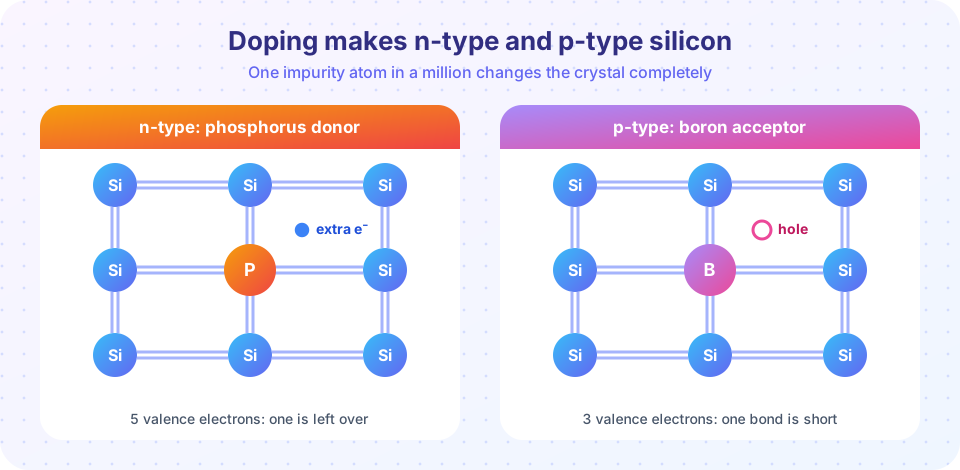
Pure silicon is a poor conductor with about 10¹⁰ carriers per cm³. Add one phosphorus atom for every five million silicon atoms and the crystal has 10¹⁶ free electrons per cm³: a million times more. Add boron instead and you get free holes. This control, by a trace of the right impurity, is what turns a crystal into an engineering material.
This chapter shows how doping works, how to calculate the carrier densities and the Fermi level that result, and how those carriers move under a field or a concentration gradient.
What you will learn
- What each lesson in the chapter covers and why the order matters.
- How a donor or an acceptor changes which carrier dominates.
- The two transport mechanisms, drift and diffusion, in one sentence each.
- The numbers that you should be able to recall: dopant range, ionization energy and the thermal-equilibrium formulas.
The big picture
Add a dopant
Carriers follow
The Fermi level moves
Carriers move
What each lesson covers
- Donors and acceptors: which atoms dope silicon, why their energy levels sit so close to a band edge, and what compensation means.
- Carriers at equilibrium: how to compute n, p and the Fermi level for a given doping, and the three temperature regimes.
- Drift and diffusion: mobility, resistivity versus doping, the diffusion current and the Einstein relation.
- Chapter review: a ten-question test and a formula sheet.
The chapter feeds directly into chapter 4: a PN junction is simply a p-type region touching an n-type region, and the current in it is a balance of drift and diffusion.
Try it
The first demo shows how small the doping is as a fraction of the crystal: slide the doping and see "one dopant per N silicon atoms".
Press Run (or Ctrl + Enter) to see the console output here.
No output.
Common misconceptions
"Doping makes silicon charged." An n-type crystal is electrically neutral: each free electron is balanced by a positively charged donor ion fixed in the lattice.
"Heavy doping means a different material." Even at 10¹⁹ cm⁻³ the crystal is still more than 99.9 percent silicon.
Check your understanding
Quick check · 4 questions
of 4 answered You scored / 4 · perfect!
-
1. Which lesson explains how to find n and p from the doping?
The equilibrium lesson combines doping, charge neutrality and n·p = ni². -
2. A phosphorus atom in silicon makes the crystal
Phosphorus has five valence electrons, so it donates one extra electron. -
3. Which two mechanisms move carriers?
A field causes drift and a concentration gradient causes diffusion. -
4. A donor-doped crystal with Nd = 10¹⁶ cm⁻³ is
Free electrons and ionized donors balance, so the crystal is neutral.
Summary
- Donors (group V) make n-type silicon; acceptors (group III) make p-type silicon.
- At equilibrium n·p = ni² still holds, with n or p set by the doping.
- The Fermi level moves toward the majority carrier's band.
- Drift (field) and diffusion (gradient) are the two current mechanisms.
Next: Donors and Acceptors: The Impurities That Dope Silicon
Track your progress
Create a free account to tick off lessons and pick up where you left off on any device.
of Semiconductor Devices lessons completed