


















Lesson 23 of 45 · Bipolar Junction Transistors
BJT structure and operation
See how an npn transistor is built and why doping, a thin base and two biased junctions make a controllable current, with band diagrams and a runnable model.
A transistor is not magic; it is a carefully proportioned stack of silicon. In this lesson you will see why the emitter is doped heavily, why the base is both thin and lightly doped, and how the voltage on the base-emitter junction decides how many carriers flow. By the end you will be able to read a band diagram of a BJT and to compute a typical saturation current from the geometry.
What you will learn
- The doping and width pattern of an npn transistor and the job of each layer.
- How forward-active biasing creates injection, transport and collection.
- What injection efficiency and base transport factor mean.
- Why the collector current is exponential in V_BE, with 60 mV per decade.
- How to estimate the saturation current I_S from device parameters.
Key terms
Minority carrier: the carrier type that is scarce in a region (electrons in a p-type base).
Injection efficiency (γ): the fraction of the emitter-junction current that is carried by the useful carriers (electrons for npn).
Base transport factor (α_T): the fraction of injected carriers that reach the collector without recombining.
Thermal voltage (V_T): kT/q, about 25.85 mV at 300 K.
Saturation current (I_S): the scale current in the exponential law, set by geometry and doping.
The layer recipe
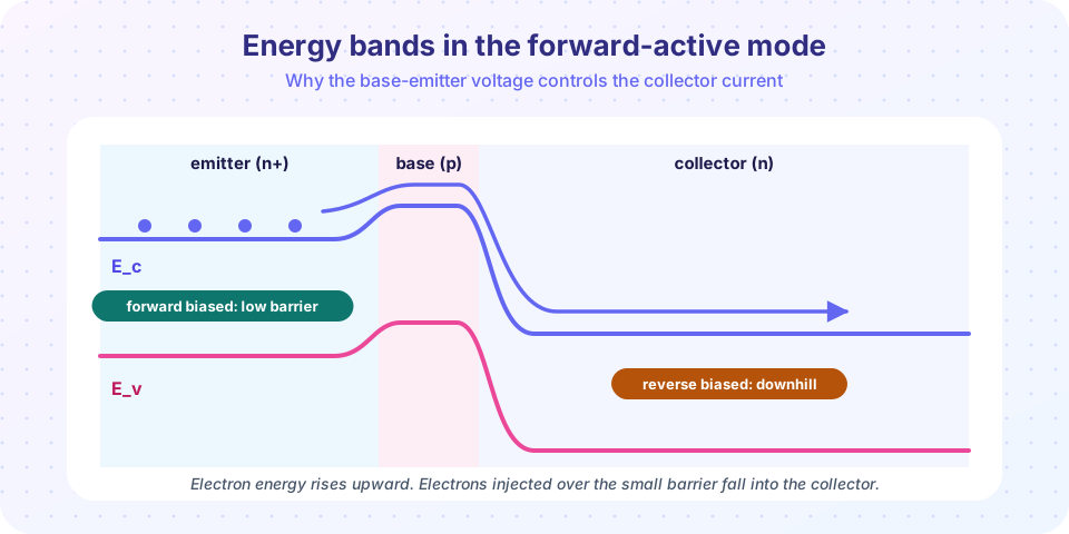
Typical doping levels for a discrete silicon npn transistor look like this.
| Layer | Doping (cm⁻³) | Width | Role |
|---|---|---|---|
| Emitter (n+) | 10¹⁹ to 10²⁰ | about 1 µm | inject many electrons, few holes |
| Base (p) | 10¹⁶ to 10¹⁸ | 0.05 to 1 µm | thin, so carriers cross it quickly |
| Collector (n) | 10¹⁵ to 10¹⁷ | several µm | lightly doped to hold a high reverse voltage |
The doping pattern is deliberately lopsided. Think of two reservoirs separated by a low wall: the emitter holds far more electrons than the base holds holes. When the wall (the barrier) is lowered by forward bias, electrons spill into the base in large numbers, while holes spill back into the emitter only in small numbers. The more lopsided the doping, the more of the emitter junction current is electrons, and the better the transistor works.
Three steps: injection, transport, collection
1. Injection. Forward bias V_BE of about 0.6 to 0.7 V lowers the barrier by qV_BE. The electron density just inside the base edge rises above its equilibrium value by the Boltzmann factor e^(V_BE / V_T). Mathematically, at the base side of the junction:
n(0) = n_p0 · e^(V_BE / V_T), with n_p0 = n_i² / N_B
where N_B is the base doping and n_i the intrinsic carrier density.
2. Transport. In the base, electrons move by diffusion. At the collector side the reverse bias keeps their density essentially zero, so the electron density falls almost linearly from n(0) to 0 across the base width W_B. A straight line of density means a constant diffusion current:
J_n = q D_n · n(0) / W_B
where D_n is the electron diffusion coefficient in the base.
3. Collection. The collector field sweeps the electrons away. The collector current is therefore
I_C = I_S · e^(V_BE / V_T), with I_S = q · A · D_n · n_i² / (N_B · W_B)
(A is the emitter area). The product N_B · W_B is the number of base dopants per unit area. Engineers call it the Gummel number. A smaller Gummel number gives a larger I_S and a higher current, but also a lower breakdown voltage and a greater risk of punch-through, so it is a trade-off.
Notice what is missing from the formula: the collector voltage. The collector junction acts only as a collector, so V_CE barely matters. (The small effect that remains, the Early effect, comes up in the next lessons.)
A worked example
Take an emitter area A = 10 µm × 10 µm = 10⁻⁶ cm², base doping N_B = 10¹⁷ cm⁻³, base width W_B = 0.1 µm = 10⁻⁵ cm, D_n = 20 cm²/s and n_i = 10¹⁰ cm⁻³ at 300 K.
I_S = (1.602e-19 · 1e-6 · 20 · 1e20) / (1e17 · 1e-5) = 3.2e-16 A
At V_BE = 0.70 V: V_BE / V_T = 0.70 / 0.02585 = 27.08, and e^27.08 ≈ 5.8e11, so I_C ≈ 3.2e-16 × 5.8e11 ≈ 0.18 mA. At V_BE = 0.60 V the exponent is 23.21, so I_C ≈ 3.8 µA. A drop of 100 mV cut the current by a factor of about 48.
Each 59.5 mV (that is, V_T · ln 10) changes the current by a factor of ten, at 300 K. This "60 mV per decade" rule is the single most useful number to remember about bipolar transistors.
Why the numbers work: injection efficiency and transport factor
Two factors reduce the ideal behavior. The emitter junction current has two parts: electrons into the base (useful) and holes back into the emitter (wasted). The injection efficiency is
γ = I_nE / (I_nE + I_pE)
and it is close to 1 when the emitter is far more heavily doped than the base. Second, a few electrons recombine in the base. The base transport factor is approximately
α_T ≈ 1 − W_B² / (2 L_n²)
where L_n = √(D_n τ_n) is the electron diffusion length. With L_n = 14 µm and W_B = 0.1 µm the loss is only 0.0025%. The common-base current gain is α = γ · α_T, and it is always just a little below 1.
Common misconceptions
"Two diodes back to back make a transistor." Wiring two separate diodes does not work, because the electrons injected by the first diode recombine in a wide middle region. The magic needs a thin, shared base so carriers cross it before recombining.
"The collector current is limited by the collector voltage." In the active region it is set by the base-emitter voltage; the collector just collects.
"The base current is what makes the collector current flow." The base current is a side effect (recombination and back-injection); the cause is the base-emitter voltage. Current gain is a convenient way of describing the result.
Try it
First, plot the exponential law for the device above. The vertical axis is logarithmic, so the 60 mV-per-decade rule appears as a straight line.
Press Run (or Ctrl + Enter) to see the result here.
Program input · what you'd type while the program runs
Type the answers before you press Run, one per line. Each time the program reads a line (with input()), it gets the next line from this box.
Second, look inside the base. The electron density falls linearly from n(0) at the emitter side to zero at the collector side. The slope is the diffusion current, so a thinner base means a steeper slope and a larger current at the same V_BE.
Press Run (or Ctrl + Enter) to see the result here.
Program input · what you'd type while the program runs
Type the answers before you press Run, one per line. Each time the program reads a line (with input()), it gets the next line from this box.
Check your understanding
Quick check · 4 questions
of 4 answered You scored / 4 · perfect!
-
1. Why is the emitter doped much more heavily than the base?
Heavy emitter doping makes electron injection into the base dominate over hole injection into the emitter, so injection efficiency is close to 1. -
2. In the active region, I_C increases by a factor of 10 when V_BE rises by about
V_T ln 10 is about 59.5 mV at 300 K, so each 60 mV adds a decade to the current. -
3. Which quantity in I_S = qA·D_n·n_i²/(N_B·W_B) makes I_S larger if it is reduced?
I_S is inversely proportional to the number of base dopants per area, the Gummel number. -
4. The electron density in the base of an ideal active BJT falls
The collector sweeps electrons away so the density there is about zero; for a short base the profile between is a straight line.
Summary
- An npn transistor is a heavily doped emitter, a thin lightly doped base and a collector that tolerates a high reverse voltage.
- Forward bias on the emitter junction injects electrons; the base transports them by diffusion; the collector junction collects them.
I_C = I_S e^(V_BE/V_T)withI_S = qAD_n n_i²/(N_B W_B); the current changes tenfold per 59.5 mV.- Injection efficiency γ and base transport factor α_T are both close to 1, so α = γ·α_T is just below 1.
Next: Currents and gain
Track your progress
Create a free account to tick off lessons and pick up where you left off on any device.
of Semiconductor Devices lessons completed