


















Lesson 17 of 45 · The PN Junction
Chapter 4 Overview: The PN Junction
Preview chapter 4: what happens when p-type meets n-type, the depletion region and built-in field, the diode equation, junction capacitance and breakdown.
Take a block of n-type silicon and a block of p-type silicon, join them, and something remarkable happens at the boundary: a thin layer empties of mobile carriers, an electric field appears with no battery attached, and the structure becomes a one-way valve for current. That structure is the PN junction. It is the simplest device in the course and the building block of nearly all the others: a bipolar transistor is two junctions, an LED is a junction that emits light, a solar cell is a junction that absorbs it.
This chapter follows the junction through four situations: at rest, under forward and reverse voltage, as a capacitor, and at breakdown.
What you will learn
- The sequence of events that creates the depletion region.
- What the four lessons of the chapter cover.
- The key numbers: built-in voltage near 0.7 V and diode knee near 0.6 to 0.7 V.
- How the junction connects to everything else in the course.
What happens when p meets n
- Gradients appear
- Diffusion
- Ions uncovered
- A field builds
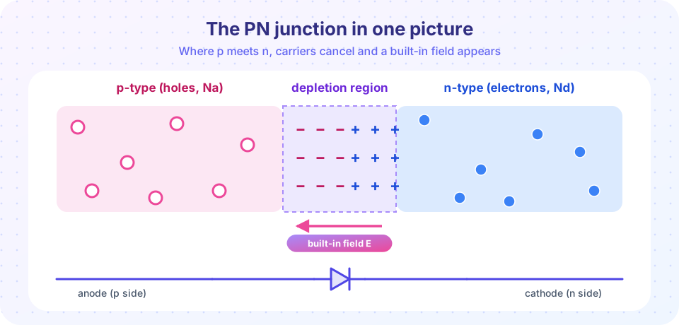
When the two sides touch, electrons diffuse from n to p and holes from p to n because each side has a huge excess of its own carrier. As they cross, they recombine with the opposite carrier, leaving behind fixed ionized dopant atoms that are no longer neutralized: positive donors on the n side, negative acceptors on the p side. Those charges produce an electric field that pushes electrons back toward n and holes back toward p. The field grows until the drift it causes exactly cancels the diffusion. In equilibrium no net current flows, and a depletion region (no mobile carriers) separates the two neutral regions.
What each lesson covers
- The junction in equilibrium: charge, field, potential and band diagram; the built-in voltage Vbi and the depletion width W.
- Diode current-voltage characteristics: forward and reverse bias, minority carrier injection, and the ideal diode equation.
- Capacitance and breakdown: depletion and diffusion capacitance, varactors, Zener and avalanche breakdown.
- Chapter review: a ten-question test and a formula sheet.
Try it
The first demo walks through the four steps above. Press a step button to see which carriers move and what appears.
Press Run (or Ctrl + Enter) to see the result here.
Program input · what you'd type while the program runs
Type the answers before you press Run, one per line. Each time the program reads a line (with input()), it gets the next line from this box.
Common misconceptions
"The built-in voltage of a junction can power a circuit." A voltmeter across an unbiased junction reads zero. The contact potentials at the metal contacts exactly cancel Vbi, as they must in equilibrium.
"The depletion region is empty of everything." It is empty of mobile carriers, not of charge: it contains the fixed ionized dopant atoms.
Check your understanding
Quick check · 4 questions
of 4 answered You scored / 4 · perfect!
-
1. What creates the depletion region?
Diffusion across the boundary leaves uncovered donor and acceptor ions, which form the depletion region. -
2. In which direction does the built-in field point?
Positive donor ions are on the n side and negative acceptor ions on the p side, so the field points from n to p. -
3. At equilibrium, the net current across the junction is
The field produces a drift current equal and opposite to the diffusion current. -
4. A bipolar transistor consists of
An npn or pnp transistor has two back-to-back PN junctions.
Summary
- Joining p and n makes carriers diffuse, leaving a depletion region of fixed ions.
- The ions create a built-in field from n to p that stops further diffusion.
- Vbi = (kT/q) ln(Na Nd/ni²), typically 0.6 to 0.9 V for silicon.
- The junction is the building block of diodes, LEDs, solar cells and transistors.
Next: The Junction in Equilibrium: Field, Potential and Depletion Width
Track your progress
Create a free account to tick off lessons and pick up where you left off on any device.
of Semiconductor Devices lessons completed