


















Lesson 38 of 45 · Fabrication and Scaling
Scaling, Moore's law and the move to 3D transistors
Understand Moore's law and Dennard scaling with numbers, why scaling slowed, what short-channel effects and high-k dielectrics are, and why FinFETs and nanosheets replaced planar MOSFETs.
For over fifty years, every couple of years chip makers found a way to put twice as many transistors on a chip. That trend, called Moore's law, together with a recipe for making transistors faster and cooler as they shrank (Dennard scaling), is the reason your phone beats a 1990s supercomputer. Around 2005 the recipe broke, and the industry has been reinventing the transistor since. This lesson explains both halves of the story with real numbers.
What you will learn
- What Moore's law actually says and how to fit it to real data.
- The rules of Dennard (constant-field) scaling and what they predict for delay and power.
- Why scaling slowed: leakage, the 60 mV/decade limit and short-channel effects.
- How high-k metal gates, strain and 3D transistors (FinFET, gate-all-around) restore gate control.
- What "technology node" names mean today.
Key terms
Moore's law: the observation that the number of transistors on a chip doubles about every two years.
Dennard scaling: shrinking dimensions and voltages by the same factor 1/κ keeps the electric field constant and power density constant.
Short-channel effect: degradation of gate control when the channel length becomes comparable to the depletion width.
DIBL (drain-induced barrier lowering): the drain voltage lowers the barrier at the source, reducing V_T.
EOT (equivalent oxide thickness): the SiO₂ thickness that would give the same capacitance as the real dielectric.
Moore's law: an economic observation
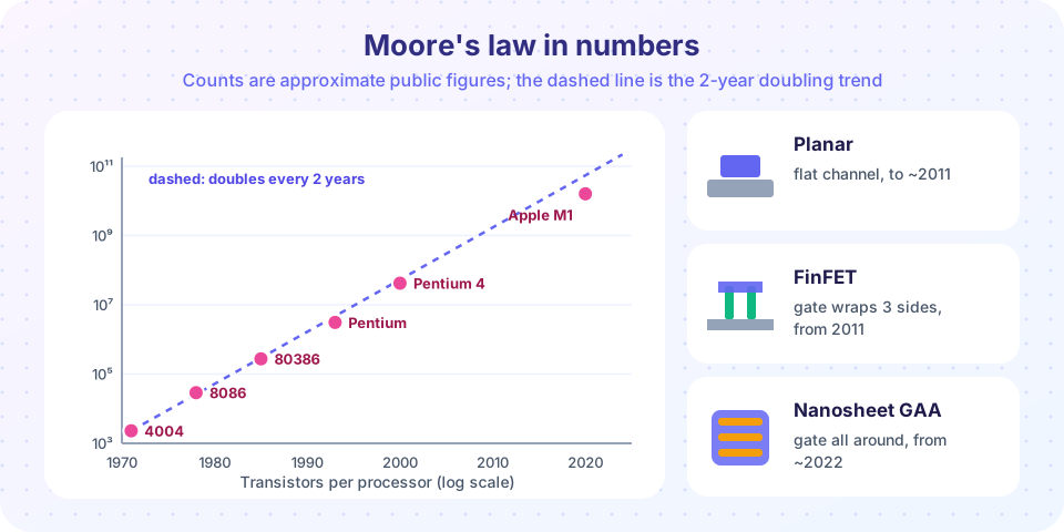
In 1965 Gordon Moore noticed that the number of components on the most economical integrated circuit had been doubling every year, and predicted that this would continue. In 1975 he revised the period to two years. It is not a law of nature; it is a self-fulfilling prophecy that the industry used as a roadmap. A rough set of public figures: Intel 4004 (1971) about 2,300 transistors; 8086 (1978) about 29,000; 80386 (1985) about 275,000; Pentium (1993) about 3.1 million; Pentium 4 (2000) about 42 million; Apple M1 (2020) about 16 billion. Fitting a straight line to log₂(count) against year gives a doubling time of about 2.2 years (the Python cell below does that fit).
Dennard scaling: shrink and win
In 1974 Robert Dennard and colleagues at IBM described how to shrink a MOSFET so that it stays well behaved. Scale all dimensions (L, W, t_ox, junction depth) and the supply voltage by 1/κ (κ > 1), and the doping by κ:
| Quantity | Factor |
|---|---|
| Length, width, oxide thickness | 1/κ |
| Supply voltage V_DD | 1/κ |
| Doping N_A | κ |
| Electric field | 1 (constant) |
| Gate capacitance C ∝ WL/t_ox | 1/κ |
| Drive current I ∝ (W/L)(V−V_T)² / t_ox | 1/κ |
| Gate delay ∝ CV/I | 1/κ |
| Power per transistor ∝ VI | 1/κ² |
| Transistor density | κ² |
| Power density (power per unit area) | 1 |
Example. A generation with κ = 1.4 (each linear dimension times 0.7) doubles the number of transistors in the same area (1.4² ≈ 2), makes each gate 1.4 times faster, and halves the power per transistor so the total power density stays the same. Faster, cheaper per transistor, and no hotter: it was an extraordinary free lunch.
Why the free lunch ended
Voltage should have shrunk with dimensions, but V_T could not. The subthreshold slope is at least 60 mV per decade at room temperature, so lowering V_T by 100 mV raises off-leakage by a factor of 10^(100/70) ≈ 27 (for S = 70 mV/decade). Designers kept V_T, and therefore V_DD, roughly fixed near 0.7 to 1 V from about 2005. With voltage stuck, the power density grows by about κ per generation, because each transistor still dissipates roughly CV² f but there are κ² more of them per area. Chips ran into a power wall: clock frequencies plateaued at 3 to 5 GHz, and extra transistors went into multiple cores, caches and accelerators instead of faster single cores.
Three further problems appeared as channels shrank below about 100 nm.
- Short-channel effects. When L is comparable to the source and drain depletion widths, the drain shares control of the channel with the gate. V_T drops (V_T roll-off), and a higher V_DS lowers it more (DIBL). Leakage rises and the transistor no longer saturates cleanly.
- Gate-oxide tunneling. Gate control needs a large C_ox, so t_ox was scaled to about 1.2 nm of SiO₂, only a few atoms thick. Electrons tunnel through, and leakage grows roughly ten-fold for each 0.2 to 0.3 nm of thinning.
- Velocity saturation and mobility loss reduce the benefit of a higher gate drive (the current grows only linearly with V_ov instead of quadratically).
Fixes: materials first, then geometry
Strained silicon (around 2003). Stretching or compressing the channel lattice increases carrier mobility by tens of percent.
High-k metal gate (Intel 45 nm, 2007). Replace SiO₂ (k = 3.9) with hafnium-based oxide (k roughly 20 to 25) and the polysilicon gate with a metal. A thicker physical layer with the same capacitance cuts tunneling. For HfO₂ with k = 20, a 3 nm film has EOT = 3 nm × 3.9/20 = 0.59 nm, which would be impossible with SiO₂ without huge leakage.
FinFET (Intel 22 nm, 2011). The channel becomes a thin vertical fin of silicon and the gate wraps over its top and two sides. More of the channel is controlled by the gate, so DIBL and leakage drop and the subthreshold slope moves toward 60 mV/decade. The width of a FinFET is set by the fin count: it uses W = 2H_fin + W_fin per fin, and you cannot choose arbitrary widths.
Gate-all-around (GAA) nanosheet transistors. The channel is a stack of horizontal ultra-thin silicon sheets, each surrounded by the gate on all four sides. This is the best electrostatic control, and sheet width can be tuned. Samsung introduced GAA at its 3 nm node in 2022, and other manufacturers have followed with their own versions. Further steps include complementary FETs (p over n stacks) and delivering power from the back side of the wafer.
A useful measure is the natural length λ, the distance over which the drain's influence decays. For a rule of thumb, a transistor behaves well when L is five or six times λ. For an illustrative planar device, λ = √((ε_Si/ε_ox) t_ox W_dep); with t_ox = 1 nm and W_dep = 20 nm, λ = √(3 × 1 × 20) = 7.7 nm, so L ≳ 40 nm. With a thin double-gate fin (t_Si = 8 nm) the scale length falls to about 3.5 nm, allowing L near 17 nm. The geometry gives control that doping and oxide thinning alone could not.
What does "3 nm" mean?
Node names stopped being a physical dimension long ago. A "3 nm" process does not contain any 3 nm feature in the sense of the old gate length; gate pitch is around 40 to 50 nm and metal pitch roughly 20 to 30 nm. The names remain as marketing labels for successive generations with roughly 1.3 to 1.6 times higher density.
Common misconceptions
"Moore's law is dead, so chips stopped improving." Transistor counts still grow, but at a slower pace per unit cost, while clock speed has been flat for many years. Gains come from parallelism, specialized hardware and packaging (chiplets, 3D stacking).
"A smaller node means a faster chip." After Dennard scaling ended, shrinking mainly gives density and efficiency; speed gains per generation are modest.
"FinFET is just a smaller MOSFET." It is a different geometry whose purpose is electrostatic control, not just size.
Try it
First fit Moore's law to the real data points from the lesson and find the doubling time.
Press Run (or Ctrl + Enter) to see the result here.
Program input · what you'd type while the program runs
Type the answers before you press Run, one per line. Each time the program reads a line (with input()), it gets the next line from this box.
Second, compare constant-field Dennard scaling with the post-2005 situation in which voltage cannot be scaled. The widget applies the rules from the table to a reference gate, so you can see where the power wall comes from.
Third, see why high-k dielectrics matter: for the same capacitance (same EOT) a high-k film can be several times thicker, which cuts tunneling leakage.
Press Run (or Ctrl + Enter) to see the result here.
Program input · what you'd type while the program runs
Type the answers before you press Run, one per line. Each time the program reads a line (with input()), it gets the next line from this box.
Check your understanding
Quick check · 5 questions
of 5 answered You scored / 5 · perfect!
-
1. In Dennard scaling with factor κ, power density
Power per transistor falls as 1/κ² while density rises as κ², so power per area is constant. -
2. A SiO₂ gate would need to be about how thick to match a 3 nm HfO₂ (k = 20) layer's capacitance?
EOT = t × 3.9/k = 3 × 3.9/20 = 0.585 nm. -
3. Why could supply voltage not keep scaling down after about 2005?
Subthreshold leakage rises tenfold for each 60 to 80 mV reduction in V_T, so V_T and V_DD stalled. -
4. A FinFET improves over a planar MOSFET mainly by
More gate-controlled surface suppresses short-channel effects and leakage. -
5. What does a '3 nm' technology node name refer to today?
Node names have been marketing labels for many years.
Summary
- Moore's law (doubling every ~2 years) is an economic observation; real data fit a doubling time near 2 years.
- Dennard scaling shrinks size and voltage by 1/κ: delay 1/κ, power per transistor 1/κ², constant power density.
- Scaling stalled when V_T and V_DD could not fall (leakage, 60 mV/decade) and short-channel effects and oxide tunneling appeared.
- Strain, high-k metal gates, FinFETs and gate-all-around nanosheets restore gate control by materials and geometry.
- Node names are labels, not lengths.
Next: Chapter review
Track your progress
Create a free account to tick off lessons and pick up where you left off on any device.
of Semiconductor Devices lessons completed