


















Lesson 7 of 45 · Crystals, Bands and Carriers
Crystal Structure: The Diamond Lattice of Silicon
Learn how silicon atoms form the diamond cubic lattice: unit cell, covalent bonds, atom density, crystal planes, defects, and why wafers are single crystals.
Silicon has 14 electrons, but only four of them, the valence electrons, take part in bonding. Each atom shares one electron with each of four neighbors, and the neighbors sit at the corners of a tetrahedron. Repeat that pattern in all directions and you get the diamond cubic lattice. This regularity is what lets us talk about energy bands, because every atom sees the same surroundings.
This lesson turns the picture into numbers you can calculate: edge length, number of atoms, bond length and density.
What you will learn
- How the diamond cubic unit cell is built and how many atoms it holds.
- How to compute atom density, bond length and mass density from the lattice constant.
- What crystal planes and Miller indices are, and why wafer orientation matters.
- The difference between single-crystal, polycrystalline and amorphous silicon, and typical defects.
Key terms
- Unit cell: the smallest repeating block of the lattice.
- Lattice constant a: the edge length of the cubic cell (0.5431 nm for Si).
- Covalent bond: a pair of shared electrons joining two atoms.
- Miller indices (hkl): three integers that name a family of crystal planes.
Bonds: four neighbors per atom
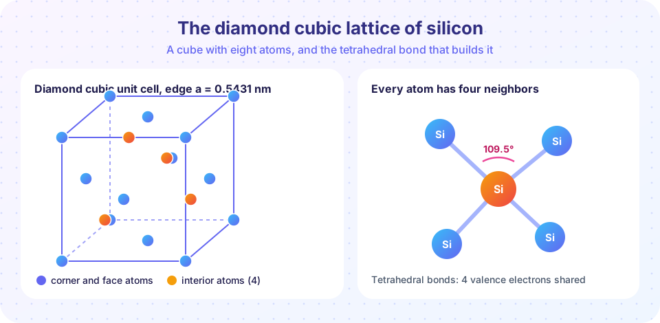
A silicon atom has four valence electrons. To fill its outer shell with eight, it shares one electron with each of four neighbors, forming four covalent bonds. The bonds repel one another and settle as far apart as possible, at about 109.5° between any two. This is the tetrahedral geometry shown in the right panel of the figure.
Each bond holds two electrons, one from each atom. At absolute zero every bond is full, no electron is free to move, and the crystal is an insulator. Free carriers appear only when an electron is knocked out of a bond.
The diamond cubic unit cell
Place atoms at the eight corners and the six face centers of a cube. That is a face-centered cubic (FCC) lattice. Now add four more atoms inside the cube, at one quarter of the way along the cube's diagonal directions, for example at (¼, ¼, ¼) in units of a. The result is the diamond cubic structure.
Count the atoms. A corner atom is shared among 8 cubes, so the 8 corners give 8 × ⅛ = 1. A face atom is shared between 2 cubes, so 6 faces give 6 × ½ = 3. The four interior atoms belong entirely to this cube. Total: 1 + 3 + 4 = 8 atoms per cell.
Silicon's lattice constant is a = 0.5431 nm (5.431 × 10⁻⁸ cm). From this we can compute:
atom density   = 8 / a³ = 8 / (5.431e-8 cm)³ ≈ 4.99e22 cm⁻³
nearest neighbor = a·√3 / 4 = 0.5431 × 1.732 / 4 ≈ 0.2352 nm
mass density   = 8 × 28.0855 g/mol / (6.022e23 /mol × a³) ≈ 2.33 g/cm³
The nearest-neighbor distance is the Si–Si bond length, 0.235 nm. Compared with the full cube, diamond lattices are open: only about 34 percent of the volume is filled by touching spheres, which is why impurity atoms can slip into the lattice.
Germanium has the same structure with a = 0.5658 nm. Gallium arsenide has a related structure called zincblende, where gallium and arsenic atoms occupy the two interleaved FCC lattices (a = 0.5653 nm).
Crystal planes and wafer orientation
A crystal looks different depending on the direction you cut it. Miller indices label the planes. The plane perpendicular to the x axis is (100), the diagonal plane parallel to the z axis is (110), and the plane that cuts all three axes at equal distances is (111).
Atoms are packed differently in each plane. For the atoms that lie in one plane of the FCC sublattice:
| Plane | Atoms per unit area | Value for silicon |
|---|---|---|
| (100) | 2 / a² | 6.8 × 10¹⁴ cm⁻² |
| (110) | 4 / (√2 a²) | 9.6 × 10¹⁴ cm⁻² |
| (111) | 4 / (√3 a²) | 7.8 × 10¹⁴ cm⁻² |
Wafer orientation matters because it changes how many dangling bonds are at the surface. Most MOS integrated circuits use (100) wafers, because the silicon-oxide interface on that plane has fewer electrically active traps. Bipolar devices often used (111) wafers.
Single crystal, poly and amorphous
Devices need single-crystal silicon, where the lattice is regular across the whole wafer. It is grown by the Czochralski method: a seed crystal is dipped into molten silicon and slowly pulled out while rotating, and a long cylinder (an ingot) of crystal grows. Sawing and polishing then give wafers.
Polycrystalline silicon (polysilicon) has many small crystal grains with boundaries between them; it is used for gates and some solar cells. Amorphous silicon has no long-range order and is used in thin-film displays and cheap solar panels.
Real crystals have defects: vacancies (missing atoms), interstitials (extra atoms between lattice sites), dislocations (line defects) and impurities. A defect can capture carriers, so manufacturers go to great lengths to avoid them. The device-grade silicon of a chip factory has impurities well below one part per billion, except for the dopants we add on purpose.
Try it
The first calculation derives silicon's density and bond length from the lattice constant alone, and compares them with Ge and GaAs.
Press Run (or Ctrl + Enter) to see the result here.
Program input · what you'd type while the program runs
Type the answers before you press Run, one per line. Each time the program reads a line (with input()), it gets the next line from this box.
Press Run (or Ctrl + Enter) to see the result here.
Program input · what you'd type while the program runs
Type the answers before you press Run, one per line. Each time the program reads a line (with input()), it gets the next line from this box.
Common misconceptions
"Silicon atoms touch like marbles in a box." The lattice is open. Only about a third of the volume is filled, which is why dopants and defects fit in.
"Any silicon works for chips." Chip-grade silicon must be single crystal with impurity levels far below what a metallurgist would call pure.
Check your understanding
Quick check · 5 questions
of 5 answered You scored / 5 · perfect!
-
1. How many atoms does the diamond cubic unit cell contain?
Corners give 1, faces give 3, and four interior atoms give 4, for a total of 8. -
2. What is the angle between the bonds of a silicon atom?
Four bonds spread as far apart as possible in a tetrahedron, 109.5° apart. -
3. Silicon's lattice constant is 0.5431 nm. What is its approximate atom density?
8 atoms per cell divided by a³ = (5.431 × 10⁻⁸ cm)³ gives about 5 × 10²² cm⁻³. -
4. Why do MOS chips usually use (100) wafers?
The lower interface trap density on (100) improves MOSFET behavior. -
5. Which description matches polysilicon?
Polysilicon consists of grains, unlike single-crystal or amorphous silicon.
Summary
- Silicon's four valence electrons make four tetrahedral covalent bonds (109.5°).
- The diamond cubic cell holds 8 atoms; a = 0.5431 nm gives about 5 × 10²² atoms per cm³ and a bond length of 0.235 nm.
- Wafer orientation matters; MOS technology favors (100).
- Devices need single-crystal material with extremely low impurity levels.
Track your progress
Create a free account to tick off lessons and pick up where you left off on any device.
of Semiconductor Devices lessons completed