


















Lesson 22 of 45 · Bipolar Junction Transistors
Chapter overview: Bipolar Junction Transistors
A map of the bipolar junction transistor chapter: how three doped layers make a current-controlled switch and amplifier, and what each lesson covers.
In the last chapter you learned how a single pn junction rectifies current. Put two junctions back to back, share the middle layer, and something remarkable happens: a small current in the middle layer controls a much larger current flowing through the whole sandwich. That sandwich is the bipolar junction transistor, or BJT. It was demonstrated at Bell Labs in 1947 (the point-contact version) and 1948 to 1951 (the junction version, thanks to William Shockley's theory), and it launched the electronics age.
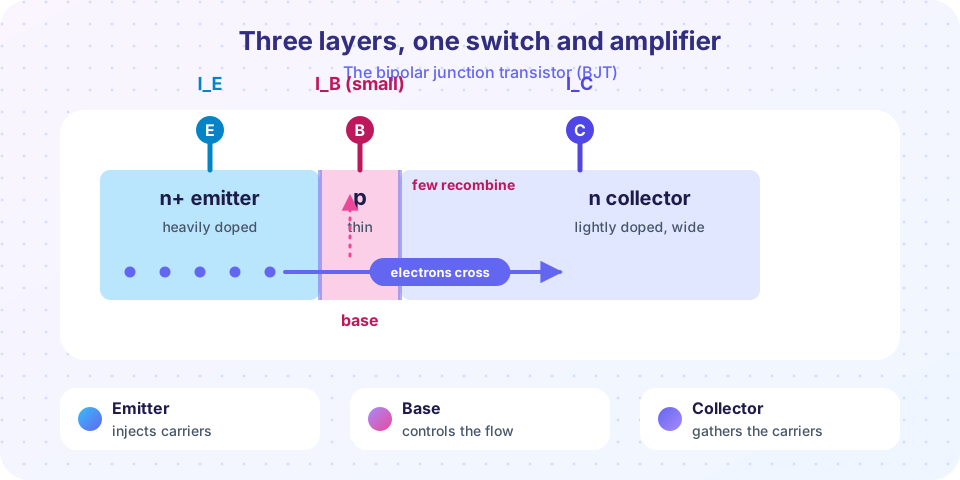
What you will learn in this chapter
- How the three layers of a BJT are doped and shaped, and why the base must be thin.
- Why the base-emitter voltage controls the collector current exponentially.
- How current gain (beta and alpha) links the three terminal currents.
- Which of the four operating regions you use for a switch and which for an amplifier.
- How to design a simple transistor switch from a handful of equations.
Key terms
Emitter: the heavily doped layer that injects carriers into the base.
Base: the thin, lightly doped middle layer that controls the flow of carriers.
Collector: the layer that collects the carriers that cross the base.
Current gain (beta): the ratio of collector current to base current, I_C / I_B.
Operating region: one of cutoff, forward-active, saturation or reverse-active, set by the bias of the two junctions.
The big picture
A BJT has three terminals and two pn junctions. In an npn transistor the layers are n, p, n; in a pnp transistor they are p, n, p. We will work with npn devices because electrons are more mobile than holes, which makes npn transistors faster; every statement carries over to pnp with the polarities reversed.
Three ideas carry the whole chapter.
- Injection. When the base-emitter junction is forward biased, the heavily doped emitter floods the base with minority carriers (electrons in an npn device).
- Transport. The base is so thin (often under a micrometer, in modern devices only tens of nanometers) that nearly every injected electron reaches the far side before it can recombine.
- Collection. The reverse-biased base-collector junction has a strong electric field that sweeps those electrons into the collector, no matter how high the collector voltage is.
The collector current therefore depends on how many electrons were injected, which depends on the base-emitter voltage, and hardly at all on the collector voltage. That is the behavior of a good controlled current source, which is the core of every amplifier.
Three layers, two junctions
Injection and collection
A small current steers a big one
Four regions
What you can build
Lessons in this chapter
- Structure and operation: doping, band diagram and why the base is thin.
- Currents and gain: the exponential law, alpha, beta and the Ebers-Moll model.
- Regions and switching: the four regions, load lines and a worked switch design.
- Chapter review: one-page recap and a long quiz.
Try it
A first taste: the widget below fixes beta at 100 and lets you set the base current. Watch how the collector current follows. It is a demonstration of the relation, not a circuit simulator.
Check your understanding
Quick check · 3 questions
of 3 answered You scored / 3 · perfect!
-
1. Which layer of an npn BJT is the most heavily doped?
A heavy emitter doping makes the emitter inject many more carriers into the base than the base injects back. -
2. Why is the base made thin?
A thin base means most minority carriers reach the collector junction, giving a high current gain. -
3. What does the reverse-biased base-collector junction do in the active region?
Its strong field collects every carrier that reaches it, so the collector current is set by the emitter injection.
Summary
- A BJT is two pn junctions sharing a thin middle layer; it has an emitter, a base and a collector.
- The emitter injects carriers, the thin base lets them through, and the collector gathers them.
- A small base current controls a much larger collector current.
- The four operating regions decide whether the BJT acts as a switch or an amplifier.
Next: Structure and operation
Track your progress
Create a free account to tick off lessons and pick up where you left off on any device.
of Semiconductor Devices lessons completed