


















Lesson 25 of 45 · Bipolar Junction Transistors
BJT operating regions, load lines and switching
Learn the four BJT operating regions, the Early effect, how a load line finds the operating point, and how to design a transistor switch with real numbers.
A BJT can act as an almost perfect open switch, a nearly closed switch, or a precise amplifier. Which behavior you get depends only on the bias of the two junctions. In this lesson you will learn the four regions, see the output characteristics that reveal them, use a load line to find the operating point, and finish with a complete switch design that drives a load from a 3.3 V logic pin.
What you will learn
- The four operating regions and the junction bias that defines each.
- The shape of the output characteristics and the Early effect.
- How to draw a load line and find the Q-point graphically and numerically.
- How to design a saturated transistor switch with a forced beta.
- Why a real switch is slow: storage time and what limits it.
Key terms
Forward-active region: base-emitter forward biased, base-collector reverse biased; the amplifier region.
Saturation: both junctions forward biased; the transistor is a closed switch with V_CE(sat) about 0.1 to 0.3 V.
Early effect: a slight rise of I_C with V_CE because the base narrows as the collector junction widens.
Load line: the straight line that the external circuit imposes on the I_C-V_CE plane.
Forced beta: the ratio I_C/I_B chosen for a saturated switch, deliberately below the transistor's real β.
Four regions from two junctions
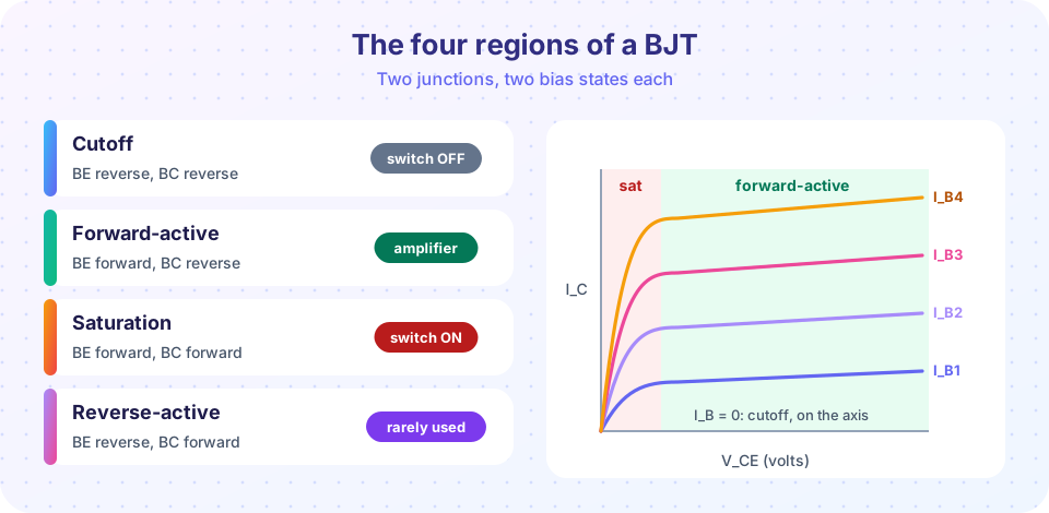
| Region | BE junction | BC junction | Use |
|---|---|---|---|
| Cutoff | reverse (or V_BE below about 0.5 V) | reverse | switch OFF, I_C is a leakage of nanoamps |
| Forward-active | forward (V_BE about 0.7 V) | reverse | amplifier |
| Saturation | forward | forward | switch ON, V_CE(sat) about 0.2 V |
| Reverse-active | reverse | forward | rarely used; low gain |
For an npn device the boundary between active and saturation is about V_CE = V_BE − 0.4 V, because the base-collector junction starts to conduct noticeably when it is forward biased by roughly 0.4 to 0.5 V. With V_BE = 0.7 V, saturation therefore begins near V_CE ≈ 0.3 V.
The Early effect
On the output characteristics (I_C against V_CE for different base currents) the curves in the active region are not perfectly flat. They tilt upward because raising V_CE widens the reverse-biased collector depletion region and shrinks the neutral base, increasing the gradient of carriers. Extend the curves backward and they meet the V_CE axis at the same point, −V_A, where V_A is the Early voltage (often 50 to 200 V). Then
I_C = I_S e^(V_BE/V_T) (1 + V_CE / V_A)
and the output resistance is r_o = (V_A + V_CE) / I_C ≈ V_A / I_C. With V_A = 100 V and I_C = 1 mA, r_o = 100 kΩ. A large r_o means a better current source.
Load lines and the Q-point
Suppose a transistor drives a collector resistor R_C from a supply V_CC. Kirchhoff's voltage law around the collector loop gives the load line
V_CE = V_CC − I_C · R_C
This is a straight line on the output characteristics, running from (V_CE = V_CC, I_C = 0) to (V_CE = 0, I_C = V_CC / R_C). The transistor must operate at a point on both the line and its own curve for the chosen I_B. That intersection is the quiescent point (Q-point).
Example. V_CC = 10 V, R_C = 2 kΩ, and a base current that gives I_C = 2 mA in the active region. Then V_CE = 10 − 2 mA × 2 kΩ = 6 V. The Q-point sits in the middle of the active region, leaving room for the output to swing both up and down: that is what you want for an amplifier. Raise I_B until I_C wants to be above V_CC / R_C = 5 mA and the transistor saturates; the load line, not β, limits I_C.
Designing a saturated switch
Goal: switch a 10 mA load from a 3.3 V logic pin, using an npn transistor with a minimum β of 100. The load is a resistor R_C connected to V_CC = 5 V.
- Collector resistor. Assume V_CE(sat) = 0.2 V.
R_C = (5 − 0.2) / 10 mA = 480 Ω(use 470 Ω, which gives about 10.2 mA). - Base current. For reliable saturation choose a forced beta of 10, far below the true β:
I_B = 10 mA / 10 = 1 mA. - Base resistor.
R_B = (3.3 − 0.7) / 1 mA = 2.6 kΩ; choose 2.4 kΩ, givingI_B = 2.6 / 2.4 k = 1.08 mA. - Check. The transistor in the active region would carry β·I_B = 108 mA, far above the 10 mA the load allows, so it is firmly saturated. Power in the transistor is
0.2 V × 10 mA = 2 mW.
The rule of thumb "forced beta of 10" costs a little extra base current but gives margin against β spread, temperature and supply variation.
Why a switch is not instant
Two effects slow switching. First, the junction capacitances must be charged through R_B. Second, in saturation both junctions inject carriers and the base fills with excess minority charge; turning the transistor off requires removing that stored charge, which adds a storage time of tens to hundreds of nanoseconds. Designers reduce it with a Baker clamp (a Schottky diode from base to collector), a lower forced beta, or by driving a negative pulse at turn-off. This is one reason why CMOS, which stores no minority charge, took over digital logic.
Common misconceptions
"Saturation means maximum amplification." It is the opposite: in saturation the transistor no longer amplifies; V_CE is stuck near 0.2 V.
"V_BE is exactly 0.7 V." It is a useful approximation for silicon at moderate current. It drops by about 2 mV per kelvin and shifts with current by 60 mV per decade.
"Using a very large base current is safe." It wastes power, increases storage time and, without a series resistor, can destroy the base-emitter junction.
Try it
The first cell draws output characteristics with the Early effect, adds the load line for V_CC = 10 V and R_C = 2 kΩ, and marks the Q-point where the curve for I_C = 2 mA crosses the line.
Press Run (or Ctrl + Enter) to see the result here.
Program input · what you'd type while the program runs
Type the answers before you press Run, one per line. Each time the program reads a line (with input()), it gets the next line from this box.
The second cell is the switch design from this lesson: it sweeps the input voltage and reports the region, using the Ebers-Moll active-region law with a saturation clamp. It is a simple behavioral model, not a SPICE simulation.
Press Run (or Ctrl + Enter) to see the result here.
Program input · what you'd type while the program runs
Type the answers before you press Run, one per line. Each time the program reads a line (with input()), it gets the next line from this box.
Check your understanding
Quick check · 5 questions
of 5 answered You scored / 5 · perfect!
-
1. Which junction biases define saturation in an npn transistor?
Saturation means the collector junction is also forward biased, so V_CE falls to about 0.2 V. -
2. A transistor has V_A = 80 V and carries I_C = 2 mA. Its output resistance is about
r_o ≈ V_A / I_C = 80 V / 2 mA = 40 kΩ. -
3. V_CC = 12 V and R_C = 3 kΩ. The maximum possible collector current, set by the load line, is
At V_CE = 0 the load line gives I_C = V_CC/R_C = 12 V / 3 kΩ = 4 mA. -
4. Why is a forced beta of about 10 used when designing a saturated switch?
Supplying far more base current than the active region would need keeps the transistor saturated even for a low-β part. -
5. What makes turning off a saturated BJT slow?
Excess minority carriers must be removed (or recombine) before the junctions return to reverse bias; this is the storage time.
Summary
- The four regions follow from junction bias: cutoff, forward-active, saturation, reverse-active.
- The Early effect gives a finite output resistance,
r_o ≈ V_A / I_C. - A load line
V_CE = V_CC − I_C R_Cfixes the Q-point together with the transistor's curve. - Switch design: choose R_C from V_CC and the load current, use a forced beta of about 10 to set I_B, then compute R_B.
- Saturation stores charge in the base, which limits switching speed.
Next: Chapter review
Track your progress
Create a free account to tick off lessons and pick up where you left off on any device.
of Semiconductor Devices lessons completed