


















Lesson 37 of 45 · Fabrication and Scaling
Chip fabrication process steps
Learn the key semiconductor fabrication steps with numbers: Deal-Grove oxidation, lithography resolution, ion implantation, diffusion, etching, deposition and planarization.
A modern chip is built from a small set of repeating operations. Each is a physical process with a simple model: oxides grow with square-root-of-time kinetics, lithography resolution follows the Rayleigh criterion, implanted dopants form a Gaussian cloud that diffusion then spreads out. In this lesson you will meet each step, compute with it and see how they combine into a patterning cycle.
What you will learn
- The growth law of thermal oxide (Deal-Grove) and how to estimate thickness.
- How photolithography prints patterns and what limits its resolution.
- How ion implantation and diffusion place and spread dopants.
- The difference between wet and dry etching, and CVD, PVD and ALD deposition.
- How chemical-mechanical planarization and copper damascene wiring finish a layer.
Key terms
Photoresist: a polymer that changes solubility when exposed to light.
Mask (reticle): the glass plate carrying one layer's pattern.
Implant dose (Φ): ions per square centimeter.
Projected range (R_p): the average depth of implanted ions.
Anisotropic etch: etches straight down, not sideways.
The patterning cycle
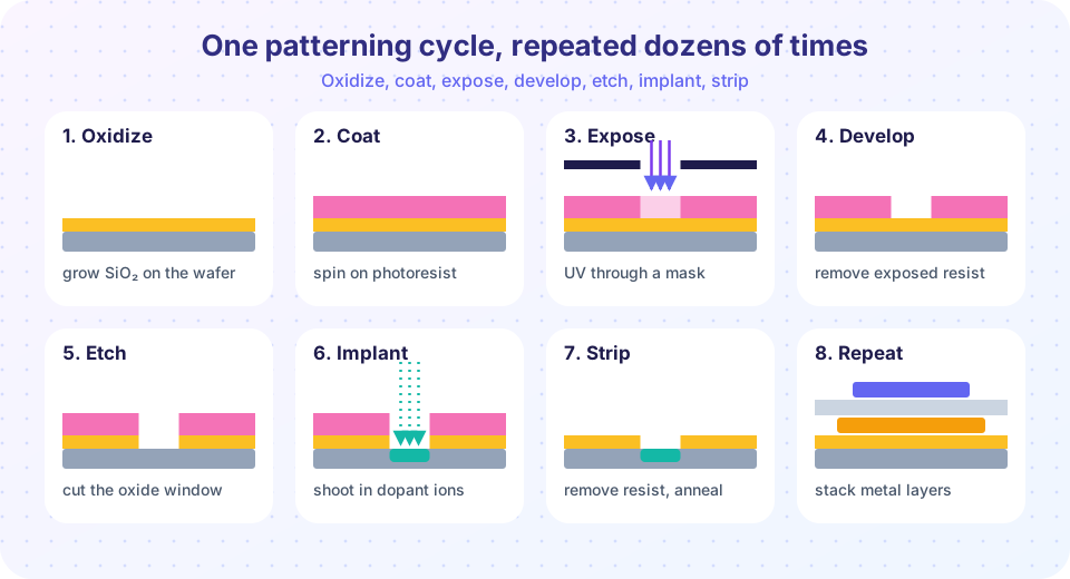
Follow one cycle in the picture.
- Oxidize. Heat silicon in oxygen or steam to grow SiO₂ on its surface.
- Coat. Spin a thin layer of photoresist on top.
- Expose. Shine ultraviolet light through a mask. Where light hits, the resist's chemistry changes.
- Develop. Wash with developer; the exposed (positive resist) areas dissolve.
- Etch. Remove the oxide where the resist is open.
- Implant. Fire dopant ions through the openings into the silicon.
- Strip. Remove the remaining resist; anneal to repair damage and activate dopants.
- Repeat. Add insulating and metal layers with the same loop.
Thermal oxidation
Silicon reacts with oxygen at 900 to 1200 °C to form silicon dioxide. As the oxide thickens, oxygen has to diffuse through it, so growth slows. The Deal-Grove model captures both reaction and diffusion:
x² + A·x = B·(t + τ)
where x is the oxide thickness, A and B depend on temperature and gas, and τ accounts for any initial oxide. The solution is
x = (A/2) [ √(1 + 4B(t + τ)/A²) − 1 ]
Two limits help your intuition. For short times (reaction-limited) x ≈ (B/A)·t: linear. For long times (diffusion-limited) x ≈ √(B t): parabolic. Typical textbook constants at 1000 °C (approximate):
| Ambient | A (µm) | B (µm²/h) | B/A (µm/h) |
|---|---|---|---|
| Dry O₂ | 0.165 | 0.0117 | 0.071 |
| Wet (steam) | 0.226 | 0.287 | 1.27 |
Example. One hour of dry oxidation at 1000 °C (τ ≈ 0): x = (0.165/2) [√(1 + 4×0.0117/0.165²) − 1] = 0.0825 × (√2.719 − 1) = 0.0825 × 0.649 = 0.054 µm = 54 nm. One hour of steam gives about 0.43 µm, eight times thicker, so thick field oxides are grown wet and thin gate oxides dry. Growing oxide consumes silicon: the silicon surface sinks by about 44% of the oxide thickness.
Photolithography
A projection scanner images the mask onto the resist at reduced size (4×). The smallest printable half-pitch follows the Rayleigh criterion
R = k₁ · λ / NA
with wavelength λ, numerical aperture NA of the lens and a process factor k₁ (practical limit about 0.25 for one exposure, achieved with tricks such as off-axis illumination and computed mask shapes). Examples:
| System | λ | NA | R for k₁ = 0.3 |
|---|---|---|---|
| ArF dry | 193 nm | 0.93 | 62 nm |
| ArF immersion (water) | 193 nm | 1.35 | 43 nm |
| EUV | 13.5 nm | 0.33 | 12 nm |
| High-NA EUV | 13.5 nm | 0.55 | 7.4 nm |
Immersion lithography puts water between the last lens and the wafer, raising NA above 1. To print finer than one exposure allows, chips use multiple patterning (several exposures per layer). EUV (extreme ultraviolet) light at 13.5 nm is absorbed by all materials, including air, so the scanner works in vacuum with mirrors rather than lenses, and the light source is a laser-heated tin plasma. Depth of focus shrinks as λ/NA², so wafers must be flat to nanometers.
Ion implantation and diffusion
To dope silicon precisely, ion implanters accelerate dopant ions (boron, phosphorus, arsenic) to energies of keV to MeV and fire them into the wafer. The ions come to rest at a depth distribution close to a Gaussian:
N(x) = Φ / (√(2π) ΔR_p) · exp( −(x − R_p)² / (2 ΔR_p²) )
with peak concentration N_p ≈ 0.4 Φ / ΔR_p. Higher energy pushes R_p deeper; dose sets the amount. Illustrative example: R_p = 0.10 µm, ΔR_p = 0.035 µm and Φ = 10¹³ cm⁻² give N_p = 0.4 × 10¹³ / (3.5×10⁻⁶ cm) = 1.1×10¹⁸ cm⁻³.
Implantation damages the lattice. An anneal (rapid thermal annealing at around 1000 °C for seconds) repairs it and lets dopants sit on lattice sites where they are electrically active. During any hot step the dopants also diffuse according to Fick's law. A Gaussian cloud keeps its shape but widens:
σ² = ΔR_p² + 2 D t
with D = D₀ exp(−E_a / kT). For boron in silicon, D₀ ≈ 0.76 cm²/s and E_a ≈ 3.46 eV (approximate), so at 1000 °C the diffusivity is about 1.5×10⁻¹⁴ cm²/s. A 30-minute drive-in has a diffusion length √(2Dt) of about 0.07 µm, which widens a 0.035 µm implant to a standard deviation of about 0.08 µm. Modern devices have such shallow junctions that the thermal budget (time at temperature) is strictly limited.
Etching, deposition and planarization
Etching removes material. Wet etching with liquid chemicals is cheap but isotropic (it undercuts the mask). Dry (plasma) etching uses reactive ions guided by an electric field to etch nearly vertically; the ratio of etch rates of two materials is the selectivity.
Deposition adds films:
- CVD (chemical vapor deposition) builds films from reacting gases (SiO₂, Si₃N₄, polysilicon); the plasma-enhanced form (PECVD) works at lower temperature.
- PVD (physical vapor deposition, sputtering) knocks atoms off a metal target onto the wafer.
- ALD (atomic layer deposition) alternates two self-limiting reactions to build a film one atomic layer at a time (about 0.1 nm per cycle), essential for high-k gate dielectrics in deep trenches.
- Epitaxy grows a new crystalline layer on the wafer.
Chemical-mechanical planarization (CMP) polishes each layer flat so the next lithography step stays in focus. In the damascene process for copper wiring (introduced by IBM in 1997), trenches are etched in the insulator, filled with copper by electroplating, and the excess is polished away. Modern chips stack 10 to 15 wiring layers.
Common misconceptions
"Lithography prints the exact size of the mask." The mask is 4 times larger and heavily pre-distorted by computation, because diffraction rounds corners and shifts edges.
"Oxide grows linearly with time." It follows x² + Ax = B(t + τ): fast at first, then slower.
"Implanted dopants are active immediately." They sit in a damaged crystal until annealing.
Try it
First, plot the Deal-Grove oxide thickness against time for dry and wet oxidation at 1000 °C and compare with the linear and parabolic limits.
Press Run (or Ctrl + Enter) to see the result here.
Program input · what you'd type while the program runs
Type the answers before you press Run, one per line. Each time the program reads a line (with input()), it gets the next line from this box.
Second, implant a boron profile and see how a drive-in anneal widens it. The code integrates the Gaussian and uses an Arrhenius diffusivity with the approximate constants quoted above.
Press Run (or Ctrl + Enter) to see the result here.
Program input · what you'd type while the program runs
Type the answers before you press Run, one per line. Each time the program reads a line (with input()), it gets the next line from this box.
Last, a Rayleigh-criterion calculator. Move the sliders to compare the lithography generations from the table.
Check your understanding
Quick check · 5 questions
of 5 answered You scored / 5 · perfect!
-
1. Oxide thickness after a long diffusion-limited growth follows approximately
In the diffusion-limited limit x² ≈ B·t, so thickness grows as the square root of time. -
2. A scanner with λ = 193 nm, NA = 1.35 and k₁ = 0.3 prints a half-pitch of about
R = 0.3 × 193 / 1.35 = 42.9 nm. -
3. Why are implanted wafers annealed?
Implants amorphize the lattice; heating restores the crystal and puts dopants on lattice sites. -
4. Which deposition method builds a film one atomic layer at a time?
Atomic layer deposition alternates self-limiting surface reactions. -
5. Why does wet etching tend to undercut the mask?
Liquid etchants attack in all directions, unlike directed plasma ions.
Summary
- Thermal oxide follows Deal-Grove:
x² + Ax = B(t + τ); steam is about 8 times faster than dry O₂ at 1000 °C. - Lithography resolution is
R = k₁λ/NA; EUV and immersion shrink λ/NA. - Implants form a Gaussian (
N_p ≈ 0.4Φ/ΔR_p); annealing activates dopants and diffusion widens the profile (σ² = ΔR_p² + 2Dt). - Etching, deposition (CVD, PVD, ALD) and CMP complete a layer; copper damascene forms the wiring.
Next: Scaling and Moore's law
Track your progress
Create a free account to tick off lessons and pick up where you left off on any device.
of Semiconductor Devices lessons completed