


















Lesson 18 of 45 · The PN Junction
The Junction in Equilibrium: Field, Potential and Depletion Width
Derive the built-in voltage Vbi, electric field and depletion width W of an abrupt PN junction with the depletion approximation, with worked numbers for silicon.
You know that a depletion region forms. Now we want numbers: how large is the built-in voltage, how wide is the depletion region, and how strong is the field? The answers follow from one simplification, the depletion approximation, and Poisson's equation from electrostatics. The mathematics is short, and the results are formulas you will use for the rest of the chapter.
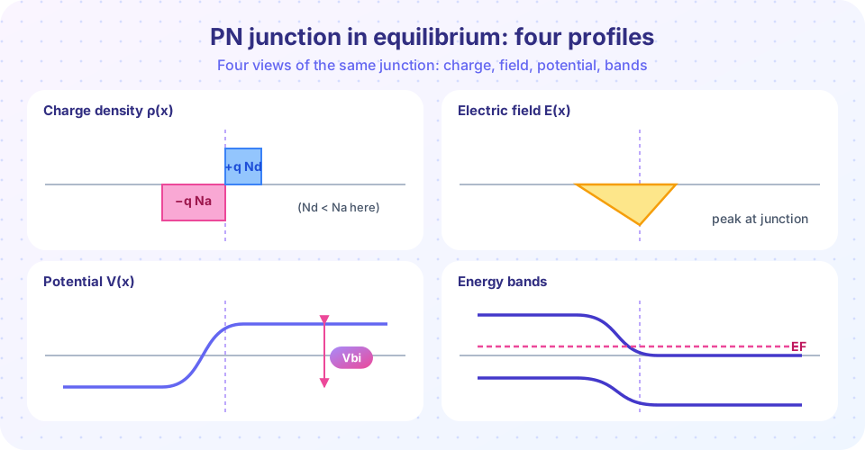
We also draw the band diagram, which shows the key fact of equilibrium: the Fermi level is flat, so the bands must bend by exactly q·Vbi.
What you will learn
- The depletion approximation and what it ignores.
- How to find Vbi from the doping and the band diagram.
- How to compute the depletion width W, the field maximum and the split between p and n sides.
- How one-sided (p⁺n or n⁺p) junctions simplify the formulas.
Key terms
- Depletion approximation: treat the depletion region as completely empty of carriers with sharp edges, and the rest as neutral.
- Built-in voltage Vbi: the potential difference across the junction in equilibrium.
- Depletion width W: the total width xp + xn of the depletion region.
- Abrupt junction: doping changes from p to n in a step.
Built-in voltage
In equilibrium the Fermi level is the same on both sides. Far from the junction, the p side has EF close to Ev and the n side has EF close to Ec. For EF to stay flat, the bands on the n side must sit lower than on the p side by the difference between those Fermi-level positions:
q·Vbi = (EF − Ei)_n + (Ei − EF)_p = kT ln(Nd/ni) + kT ln(Na/ni)
Vbi = (kT/q) · ln( Na · Nd / ni² )
For Na = 10¹⁷ and Nd = 10¹⁶ cm⁻³ in silicon at 300 K (ni = 10¹⁰ cm⁻³):
Vbi = 0.02585 × ln(10³³ / 10²⁰) = 0.02585 × ln(10¹³) = 0.02585 × 29.93 ≈ 0.77 V
Vbi is always below Eg/q (1.12 V), because the Fermi level cannot go outside the gap. It grows only logarithmically with doping, so typical silicon junctions have Vbi between 0.6 and 0.9 V.
The depletion approximation
Assume the depletion region extends from −xp (on the p side) to +xn (on the n side), with the junction at x = 0. Inside it, no mobile carriers exist, so the charge density is only that of the ionized dopants:
ρ(x) = −q Na   for −xp < x < 0
ρ(x) = +q Nd   for 0 < x < xn
ρ(x) = 0       outside (neutral)
Since the total charge must be zero (neutral device), the charges on the two sides are equal: Na·xp = Nd·xn. The heavier-doped side has the narrower depletion layer.
Poisson's equation, dE/dx = ρ/ε, integrates once to give the field:
E(x) = −q Na (x + xp) / ε    for −xp < x < 0
E(x) = −q Nd (xn − x) / ε    for 0 < x < xn
The field is negative (pointing from n to p) and peaks at x = 0:
Emax = q Nd xn / ε = q Na xp / ε
Integrating the field once more gives the potential. The total potential drop is the area of the triangular field profile, which must equal Vbi:
Vbi = (1/2) · Emax · W
Combine the pieces (W = xp + xn, charge balance, and Emax) to get the depletion width:
W = √( (2 ε Vbi / q) · (1/Na + 1/Nd) )
xn = W · Na / (Na + Nd)        xp = W · Nd / (Na + Nd)
Emax = 2 Vbi / W
Here ε = εr ε₀ = 11.7 × 8.854 × 10⁻¹⁴ F/cm = 1.036 × 10⁻¹² F/cm for silicon.
Worked example
Na = 10¹⁷ cm⁻³, Nd = 10¹⁶ cm⁻³, Vbi = 0.77 V:
1/Na + 1/Nd = 1.1e-16 cm³
2 ε Vbi / q = 2 × 1.036e-12 × 0.77 / 1.602e-19 = 9.96e6
W = √(9.96e6 × 1.1e-16) = √(1.096e-9) = 3.3e-5 cm = 0.33 µm
xn = 0.33 × 10¹⁷ / (1.1 × 10¹⁷) = 0.30 µm      xp = 0.03 µm
Emax = 2 × 0.77 / 3.3e-5 = 4.7e4 V/cm
The depletion region is a third of a micrometer wide, almost entirely on the lightly doped (n) side, and the field is about 47 kV/cm.
One-sided junctions
If one side is far more heavily doped (a p⁺n junction, Na ≫ Nd), the depletion region lies almost entirely in the lightly doped side and the formulas simplify:
W ≈ √(2 ε Vbi / (q Nd))
The junctions inside real devices are often one-sided: the emitter of a bipolar transistor and the source and drain of a MOSFET are heavily doped, and the substrate or base is lightly doped. Then only the light doping matters for W.
Try it
The first example computes all the equilibrium quantities and plots the four profiles of the figure above for your doping values.
Press Run (or Ctrl + Enter) to see the result here.
Program input · what you'd type while the program runs
Type the answers before you press Run, one per line. Each time the program reads a line (with input()), it gets the next line from this box.
Press Run (or Ctrl + Enter) to see the console output here.
No output.
Common misconceptions
"The depletion region is symmetric." It is symmetric only when Na = Nd. The more lightly doped side takes most of the width, because Na·xp = Nd·xn.
"The field in the depletion region is uniform." It is a triangle: zero at the edges and maximum at the metallurgical junction.
Check your understanding
Quick check · 5 questions
of 5 answered You scored / 5 · perfect!
-
1. The built-in voltage of a silicon junction with Na = Nd = 10¹⁶ cm⁻³ is about
Vbi = 0.02585 × ln(10³²/10²⁰) = 0.02585 × 27.6 ≈ 0.71 V. -
2. In the depletion approximation, which relation holds?
Charge neutrality requires equal charge magnitudes on the two sides, so Na·xp = Nd·xn. -
3. Where is the electric field largest?
The field grows linearly with distance through each side's charge and peaks at the junction. -
4. In a p⁺n junction (Na ≫ Nd), the depletion region lies mostly
Na xp = Nd xn means xn ≫ xp when Na ≫ Nd. -
5. Why does Vbi grow only slowly with doping?
Vbi = (kT/q) ln(Na Nd/ni²): ten times more doping adds only about 60 mV per side.
Summary
- Vbi = (kT/q) ln(Na Nd / ni²) < Eg/q; the bands bend by qVbi while EF stays flat.
- Depletion approximation: Na xp = Nd xn, triangular field, Emax = 2 Vbi / W.
- W = √((2 ε Vbi / q)(1/Na + 1/Nd)); the lightly doped side takes most of the width.
- Silicon example: 0.33 µm wide, 47 kV/cm peak field.
Track your progress
Create a free account to tick off lessons and pick up where you left off on any device.
of Semiconductor Devices lessons completed