


















Lesson 30 of 45 · MOS Capacitors and MOSFETs
MOSFET small-signal behavior, subthreshold slope and CMOS
Learn g_m and r_o for MOSFET amplifiers, the 60 mV per decade subthreshold limit and leakage, and how a CMOS inverter works with a worked power calculation.
The square-law current equations describe where a MOSFET sits; to amplify a signal or to judge leakage you need three more ideas: the small-signal parameters g_m and r_o, the way current behaves below threshold, and how two complementary transistors form a logic gate. This lesson covers all three and ends with the arithmetic behind the power consumption of a digital chip.
What you will learn
- How to compute g_m and r_o from the DC operating point and the voltage gain of a common-source stage.
- Why a MOSFET gives less transconductance than a BJT at the same current.
- What the subthreshold slope is, why it cannot beat 60 mV/decade at room temperature and what it means for leakage.
- How a CMOS inverter works, its voltage transfer curve and its noise margins.
- How dynamic power P = αCV²f follows from charging capacitors.
Key terms
Transconductance (g_m): dI_D/dV_GS at the operating point.
Output resistance (r_o): dV_DS/dI_D in saturation, 1/(λI_D).
Subthreshold slope (S): the gate voltage needed to change I_D by a factor of 10 below threshold, in mV/decade.
Switching threshold (V_M): the input voltage at which V_out = V_in on the inverter curve.
Noise margin: how much noise on a logic level a gate can tolerate without misreading it.
Small-signal parameters
Differentiate the saturation current I_D = ½ k V_ov² with respect to V_GS:
g_m = k V_ov = 2 I_D / V_ov = √(2 k I_D)
Three equivalent forms are useful: use k V_ov when you know the overdrive, 2I_D/V_ov when you know current and overdrive, and √(2kI_D) when you know current and device size.
Example. With k = 1.38 mA/V² and I_D = 0.5 mA, V_ov = √(2 × 0.5 / 1.38) = 0.851 V and g_m = 1.38 × 0.851 = 1.17 mS. A BJT at the same 0.5 mA has g_m = I_C/V_T = 19.3 mS, about 16 times more. The reason is the difference between a quadratic and an exponential law: a BJT's g_m grows linearly with current, a MOSFET's grows only as the square root. That is why bipolar transistors remain popular for high-gain, low-noise analog front ends.
The output resistance is r_o = 1/(λ I_D). A common-source amplifier with a drain resistor R_D has small-signal voltage gain
A_v = −g_m (R_D ∥ r_o)
where ∥ means "in parallel with". With g_m = 1.17 mS, R_D = 10 kΩ and r_o = 40 kΩ the parallel resistance is 8 kΩ, so A_v = −1.17 mS × 8 kΩ = −9.4. The intrinsic gain of the transistor, g_m·r_o = 2/(λ V_ov), is the maximum you can obtain from one device; it shrinks as channels get shorter.
Subthreshold: the transistor is not perfectly off
Below threshold the surface is weakly inverted and the current is a diffusion current, exponential in the gate voltage, much like a BJT:
I_D ∝ e^((V_GS − V_T) / (n V_T)), with n = 1 + C_dep / C_ox
The subthreshold slope is therefore
S = n · V_T · ln 10 = n × 59.5 mV/decade at 300 K
The factor n is at least 1 (perfect gate control), giving the famous limit of 59.5 mV, about 60 mV, per decade. For the lesson's example device C_dep = ε_Si / W_max = 1.0e-7 F/cm² and C_ox = 3.45e-7 F/cm², so n = 1.29 and S ≈ 77 mV/decade.
Now translate that into leakage. To turn the device off from V_GS = V_T = 0.34 V to V_GS = 0 V the current falls by 0.34 / 0.077 = 4.4 decades, a factor of about 27,000. With billions of transistors, an off-current of even a few nanoamperes per device would add up to amperes of leakage. Designers cannot simply lower V_T to gain speed, because each 60 to 80 mV of V_T reduction multiplies off-leakage by about ten. Thinner oxides and multi-gate structures (FinFET, gate-all-around, covered in chapter 8) move n toward 1.
The CMOS inverter
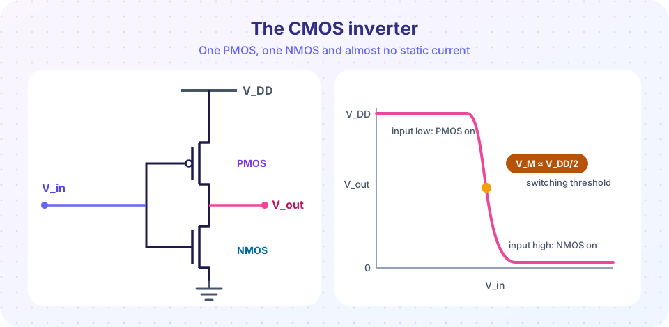
A CMOS inverter has a PMOS transistor between V_DD and the output, and an NMOS between the output and ground; both gates receive the input. Think through the cases.
- V_in = 0 V (low). The NMOS is off (V_GS = 0), the PMOS is on (V_SG = V_DD). The PMOS pulls V_out up to V_DD. No DC current flows because the NMOS is off.
- V_in = V_DD (high). The PMOS is off, the NMOS is on, V_out = 0 V. Again no DC current.
- V_in near V_DD/2. Both are on and both are in saturation for a moment. Gain is very high here (tens in real circuits; this idealized model gives over 100), which makes the output transition steep, and a short pulse of "crowbar" current flows from supply to ground.
For matched transistors (equal k and |V_T|) the switching threshold is V_M = V_DD/2. If they are not matched, with r = √(k_n/k_p):
V_M = (V_DD + V_Tp + r V_Tn) / (1 + r) (V_Tp is negative)
A high noise margin is a big reason CMOS was adopted: both logic levels are the full supply rails, so noise margins are close to V_DD/2.
Why power is low and where it goes
In a steady state one transistor is off, so static power is just leakage. The power that matters is dynamic: each time the output switches from 0 to V_DD, the load capacitance C_L is charged through the PMOS, drawing charge Q = C_L V_DD from the supply and dissipating ½ C_L V_DD² as heat in the transistor; the other half is stored on the capacitor and dissipated in the NMOS at discharge. Per full cycle E = C_L V_DD². With switching activity α (the fraction of cycles with a transition) and clock frequency f:
P_dyn = α C_L V_DD² f
Example. C_L = 1 fF, V_DD = 0.8 V, f = 3 GHz and α = 0.1 give P = 0.1 × 1e-15 × 0.64 × 3e9 = 0.19 µW per gate. The V_DD² term shows why chip designers lowered the supply voltage from 5 V to below 1 V: halving V_DD cuts dynamic power by four. A billion such gates all switching at that rate would draw 190 W, so real chips use clock gating and keep activity low.
Common misconceptions
"A CMOS gate uses no power." Only static dissipation is tiny. Dynamic power from charging capacitors and subthreshold leakage dominate in modern chips.
"Subthreshold current is only noise." It is a real, exponential current and a major source of standby power; also the basis of ultra-low-power analog circuits that operate deliberately below threshold.
"Higher g_m always requires a bigger current." For a MOSFET you can also raise g_m by increasing W/L (more k) at the same current, at the cost of area and capacitance.
Try it
Compute and plot the inverter transfer curve numerically by balancing the NMOS and PMOS currents, then find the switching threshold and the noise margins from the points where the gain equals −1.
Press Run (or Ctrl + Enter) to see the result here.
Program input · what you'd type while the program runs
Type the answers before you press Run, one per line. Each time the program reads a line (with input()), it gets the next line from this box.
Next, the subthreshold slope. The plot shows log I_D against V_GS for several gate-control factors n. The ideal n = 1 curve is steepest; the horizontal distance between two decades is S.
Press Run (or Ctrl + Enter) to see the result here.
Program input · what you'd type while the program runs
Type the answers before you press Run, one per line. Each time the program reads a line (with input()), it gets the next line from this box.
Check your understanding
Quick check · 5 questions
of 5 answered You scored / 5 · perfect!
-
1. I_D = 1 mA and V_ov = 0.2 V in saturation. The transconductance g_m is
g_m = 2 I_D / V_ov = 2 mA / 0.2 V = 10 mS. -
2. The smallest possible subthreshold slope of a conventional MOSFET at 300 K is about
S = n V_T ln 10 with n ≥ 1 gives 59.5 mV/decade at 300 K. -
3. In a CMOS inverter with a low input, which transistor is on?
A low input gives the PMOS a large source-gate voltage, so it pulls the output up; the NMOS is off. -
4. Halving V_DD while keeping C, α and f fixed changes the dynamic power by a factor of
P = αCV²f is proportional to V_DD², so halving V_DD gives one quarter. -
5. For a MOSFET versus a BJT at the same current, the transconductance is generally
g_m = I_C/V_T for a BJT (about 39 mS/mA); for a MOSFET it is 2I_D/V_ov, which is much smaller when V_ov is hundreds of millivolts.
Summary
g_m = kV_ov = 2I_D/V_ov = √(2kI_D)andr_o = 1/(λI_D); a common-source stage has gain−g_m(R_D ∥ r_o).- A MOSFET has lower g_m per milliamp than a BJT.
- Subthreshold current falls by one decade per
S = n × 59.5 mVat 300 K; leakage is the price of a low V_T. - A CMOS inverter has no DC path in a steady state; its switching threshold is V_DD/2 when matched.
- Dynamic power is
P = αC_LV_DD²f, so lowering V_DD pays off quadratically.
Next: Chapter review
Track your progress
Create a free account to tick off lessons and pick up where you left off on any device.
of Semiconductor Devices lessons completed