


















Lesson 13 of 45 · Doping and Conduction
Donors and Acceptors: The Impurities That Dope Silicon
Learn how phosphorus, arsenic and boron dope silicon, why donor and acceptor levels lie close to a band edge, how ionization works and what compensation means.
Silicon sits in group IV of the periodic table with four valence electrons. Replace a silicon atom with a group V atom (five valence electrons) and one electron has no bond to join: it is only loosely held and easily set free. Replace it with a group III atom (three valence electrons) and one bond is short of an electron: a neighbor's electron can fill it, leaving a hole somewhere else.
These two operations are the basis of all semiconductor devices. This lesson explains the atoms involved, the energy levels they create, and the simple model that predicts how loosely they hold their extra charge.
What you will learn
- Which elements act as donors and which as acceptors in silicon.
- Why the extra electron is bound by only a few tens of meV, using a hydrogen-like model.
- What complete ionization means at room temperature.
- How compensation and concentration ranges work in practice.
Key terms
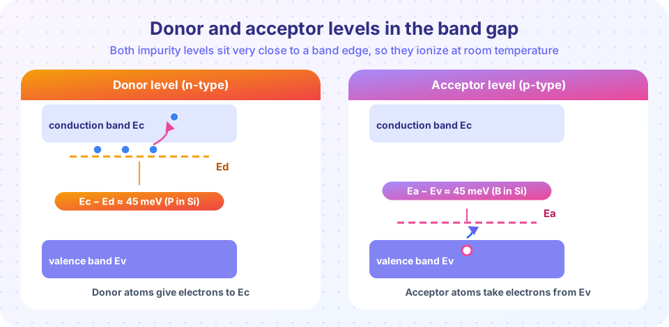
- Donor: an impurity atom that gives an electron to the conduction band; it becomes a positive ion (Nd⁺).
- Acceptor: an impurity atom that takes an electron from the valence band, creating a hole; it becomes a negative ion (Na⁻).
- Ionization energy: the energy to free the extra electron (or hole) from the impurity.
- Compensation: the presence of both donors and acceptors, which partly cancel each other.
The common dopants
In silicon the main donors are phosphorus (P), arsenic (As) and antimony (Sb). The main acceptor is boron (B); aluminum, gallium and indium are used less often.
| Dopant | Group | Role | Ionization energy in Si (meV) |
|---|---|---|---|
| Phosphorus | V | donor | 45 |
| Arsenic | V | donor | 54 |
| Antimony | V | donor | 39 |
| Boron | III | acceptor | 45 |
| Aluminum | III | acceptor | 57 |
| Gallium | III | acceptor | 65 |
| Indium | III | acceptor | 160 |
Concentrations range from about 10¹⁴ cm⁻³ (a lightly doped substrate) to above 10²⁰ cm⁻³ (the source and drain of a MOSFET), limited by how much dopant dissolves in the crystal, the solid solubility (around 10²¹ cm⁻³ for arsenic).
Why the ionization energy is so small
A hydrogen atom has one electron bound to one proton, and its ionization energy is 13.6 eV. A donor atom is similar: a positive ion core (the impurity with its four bonding electrons) holds the fifth electron. Two things make it far weaker than hydrogen:
- The crystal screens the ion's charge: the electric force is divided by the relative permittivity εr = 11.7 of silicon.
- The electron moves with the effective mass m*, not the free mass.
The hydrogen-like estimate is therefore:
E_ion = 13.6 eV × (m*/m₀) / εr²
With m*/m₀ = 0.26 and εr = 11.7, this gives about 26 meV, within a factor of two of the measured 45 meV (the model ignores details near the impurity's core). The electron's orbit radius also scales: a = 0.0529 nm × εr / (m*/m₀) ≈ 2.4 nm, wide enough to enclose many silicon atoms, which is why the macroscopic parameters εr and m* are legitimate.
Because kT = 25.9 meV at 300 K, a binding energy of 45 meV is only about 1.7 kT, so thermal energy frees most of the extra electrons. Acceptors work the same way for holes.
Complete ionization
At room temperature essentially every donor in a silicon crystal doped to 10¹⁶ cm⁻³ has given up its electron. We write:
n ≈ Nd     (n-type, complete ionization, Nd ≫ ni)
p ≈ Na     (p-type)
At very low temperature this fails: carriers "freeze out" and return to the dopants. At very high temperature, thermally generated pairs swamp the dopant electrons and the crystal turns intrinsic. Between these extremes lies the useful working range, where carrier density equals the doping, which is the extrinsic region. Lesson 3 plots all three.
Compensation
If a crystal contains both donors and acceptors, they neutralize one another: acceptors capture electrons that donors released. When Nd > Na the crystal is n-type with a net concentration Nd − Na (and the carrier mobility is reduced because all those ions scatter). The reverse gives p-type. Doping a region of the same crystal with the opposite type is exactly how junctions are made: implant boron into n-type silicon heavily enough that Na > Nd and the region flips to p-type.
How dopants get in
- Diffusion: heat the wafer in a furnace with the dopant source; atoms spread in from the surface.
- Ion implantation: accelerate dopant ions and shoot them into the wafer with precise energy and dose; a following anneal repairs damage and puts the atoms on lattice sites so they become electrically active.
- Epitaxy: grow a new crystal layer with dopants mixed in.
Chapter 8 returns to these steps.
Try it
The first example applies the hydrogen-like model to electrons and holes in silicon and germanium. It is an order-of-magnitude estimate.
Press Run (or Ctrl + Enter) to see the result here.
Program input · what you'd type while the program runs
Type the answers before you press Run, one per line. Each time the program reads a line (with input()), it gets the next line from this box.
Common misconceptions
"An n-type crystal contains extra electrons added from outside." No electrons are added. Each donor atom brings its own extra electron, and the crystal stays neutral.
"The ionization energy of a donor is like the 13.6 eV of hydrogen." The dielectric screening and small effective mass reduce it by a factor of about 300.
Check your understanding
Quick check · 5 questions
of 5 answered You scored / 5 · perfect!
-
1. Which element is a common acceptor in silicon?
Boron has three valence electrons and is the main p-type dopant. -
2. Why is the donor ionization energy only about 45 meV?
The binding energy scales as m*/(m₀ εr²), which reduces 13.6 eV by a factor of about 300. -
3. At 300 K, with Nd = 10¹⁶ cm⁻³ in silicon, the electron density is about
Donors are fully ionized, so n ≈ Nd. -
4. A crystal has Nd = 5 × 10¹⁶ cm⁻³ and Na = 2 × 10¹⁶ cm⁻³. What is the net doping?
Compensation leaves Nd − Na = 3 × 10¹⁶ cm⁻³, and donors dominate, so the crystal is n-type. -
5. How is a controlled dose of dopant placed deep into a wafer with energy control?
Ion implantation accelerates dopant ions to a chosen energy and dose; an anneal then activates them.
Summary
- Group V atoms (P, As, Sb) are donors; group III atoms (B and others) are acceptors.
- Their levels lie about 40–65 meV from a band edge (except In at 160 meV), so they ionize at 300 K.
- Hydrogen-like model: E_ion = 13.6 eV (m*/m₀)/εr² gives the right order of magnitude.
- Donors and acceptors compensate; the net doping decides the type.
Track your progress
Create a free account to tick off lessons and pick up where you left off on any device.
of Semiconductor Devices lessons completed