


















Lesson 20 of 45 · The PN Junction
Junction Capacitance and Breakdown
Learn depletion and diffusion capacitance of a PN junction, how varactors use C-V, and the two reverse breakdown mechanisms: Zener tunneling and avalanche.
A reverse-biased junction stores charge: ionized dopants on both sides of the depletion region act like the plates of a capacitor, and the plates move farther apart as the reverse voltage rises. A forward-biased junction stores charge too: injected minority carriers waiting to recombine. These capacitances limit how fast a diode can switch and make useful tunable components called varactors.
And if the reverse voltage grows large enough, the junction breaks down. Breakdown is not always destructive; a diode designed for it makes a voltage reference. We look at both mechanisms.
What you will learn
- How to compute the depletion capacitance and plot C versus VR.
- How a C-V measurement yields the doping and the built-in voltage.
- What diffusion capacitance is and when it matters.
- The difference between Zener and avalanche breakdown and their temperature behavior.
Key terms
- Depletion (junction) capacitance Cj: capacitance from the changing depletion charge, Cj = εA/W.
- Diffusion capacitance Cd: capacitance from stored minority carriers in forward bias.
- Varactor: a diode designed for its voltage-dependent capacitance.
- Breakdown voltage VBR: reverse voltage at which the current rises sharply.
Depletion capacitance
A reverse bias VR increases the barrier to Vbi + VR, so the depletion width becomes
W(VR) = √( (2 ε (Vbi + VR) / q) · (1/Na + 1/Nd) )
The charge on one side of the junction is Q = q A Nd xn, and the small-signal capacitance dQ/dV equals that of a parallel-plate capacitor with plate spacing W:
Cj = ε A / W = A · √( q ε Na Nd / (2 (Na + Nd)(Vbi + VR)) )
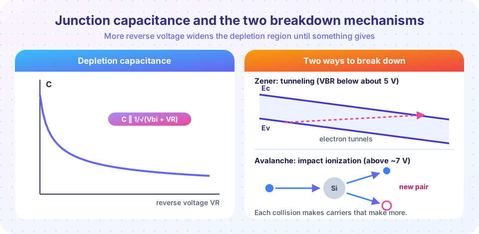
For a one-sided junction with a lightly doped side N, this simplifies to Cj = A √(q ε N / (2 (Vbi + VR))). The capacitance varies as (Vbi + VR)^(−1/2): quadruple the reverse voltage and the capacitance halves. In practice engineers write
Cj(VR) = Cj0 / (1 + VR/Vbi)^m
with m = 1/2 for abrupt junctions, 1/3 for linearly graded ones and up to 2 for hyperabrupt junctions designed for extra tuning range.
A measurement trick
Because 1/Cj² = 2 (Vbi + VR) / (q ε N A²) is a straight line in VR, plotting 1/C² against VR gives the doping from the slope and Vbi from where the line crosses zero. This C-V profiling is a standard way to measure doping in a real diode.
Varactors
In a radio tuner, a varactor diode sits in an LC circuit; the tuning voltage changes its capacitance, which changes the resonant frequency f = 1/(2π√(LC)). A capacitance ratio of about 3 to 10 over the voltage range is typical.
Diffusion capacitance
In forward bias the stored charge of injected minority carriers is Q = I τ (current times lifetime), so the incremental capacitance is
Cd = τ · I / VT
For τ = 1 µs and I = 1 mA this is 39 nF, far larger than the depletion capacitance (picofarads), which is why diodes switch off slowly after conducting: the stored charge must be removed first. Fast switching diodes reduce τ with gold doping or use Schottky junctions, which have no minority carrier storage.
Breakdown
Beyond a critical reverse voltage VBR, the current rises almost vertically. Two mechanisms are responsible:
Zener breakdown (tunneling). In heavily doped junctions, the depletion region is so thin (a few nm to tens of nm) and the field so strong (above about 10⁶ V/cm) that valence electrons on the p side can tunnel directly through the gap into the conduction band on the n side. It dominates for breakdown voltages below roughly 4Eg/q, about 4.5 V in silicon.
Avalanche breakdown (impact ionization). In lighter doping, the depletion region is wide, and carriers entering it accelerate to high energy. A carrier with enough energy collides with a lattice atom and knocks loose a new electron-hole pair, and both the new carriers accelerate and ionize others: a chain reaction. This dominates above about 6Eg/q, around 7 V in silicon, and the breakdown voltage grows as the doping falls. For a one-sided abrupt silicon junction an empirical formula is
VBR ≈ 60 V × (Eg / 1.1 eV)^(3/2) × (N / 10¹⁶ cm⁻³)^(−3/4)
where N is the doping of the lighter side. The peak field at breakdown is about 3 to 5 × 10⁵ V/cm.
The two mechanisms respond oppositely to temperature. Higher temperature makes carriers collide more with the lattice and lose energy before they can ionize, so avalanche VBR rises with temperature (positive coefficient). The band gap shrinks with temperature, which helps tunneling, so Zener VBR falls (negative coefficient). Diodes designed at about 5 to 6 V mix both and have a near-zero temperature coefficient, which is why the common 5.6 V Zener is a good voltage reference.
Try it
The first example generates synthetic C-V data for a diode with unknown doping, then recovers the doping and Vbi from the 1/C² line, exactly as in the lab.
Press Run (or Ctrl + Enter) to see the result here.
Program input · what you'd type while the program runs
Type the answers before you press Run, one per line. Each time the program reads a line (with input()), it gets the next line from this box.
Press Run (or Ctrl + Enter) to see the result here.
Program input · what you'd type while the program runs
Type the answers before you press Run, one per line. Each time the program reads a line (with input()), it gets the next line from this box.
Common misconceptions
"Breakdown destroys a diode." The breakdown process itself is not harmful; heat from too much current times voltage is. Zener and avalanche diodes are built to operate in breakdown with a current limiting resistor.
"All breakdown is the Zener effect." Most diodes named "Zener" above about 7 V actually break down by avalanche.
Check your understanding
Quick check · 5 questions
of 5 answered You scored / 5 · perfect!
-
1. How does the depletion capacitance of an abrupt junction change when reverse voltage is quadrupled (Vbi ≪ VR)?
Cj ∝ (Vbi + VR)^(−1/2), so quadrupling VR halves C. -
2. What straight line gives the doping of a one-sided junction?
1/C² = 2(Vbi + VR)/(q ε N A²): its slope gives N and its intercept gives Vbi. -
3. Which mechanism dominates breakdown in a lightly doped silicon junction of several hundred volts?
Wide depletion regions let carriers gain enough energy to ionize atoms. -
4. The temperature coefficient of avalanche breakdown voltage is
At higher temperature carriers lose energy to lattice scattering before ionizing, so a larger field is needed. -
5. Why do diodes switch off slowly after conducting?
Cd = τI/VT represents the charge that must recombine or be swept out.
Summary
- Cj = εA/W ∝ (Vbi + VR)^(−1/2) for an abrupt junction; 1/C² versus VR is a straight line giving N and Vbi.
- Varactors exploit the C-V dependence for tuning.
- Forward bias adds diffusion capacitance Cd = τI/VT.
- Zener (tunneling) breakdown is low-voltage with negative temperature coefficient; avalanche breakdown is higher-voltage with positive coefficient.
- VBR ≈ 60 V (N/10¹⁶ cm⁻³)^(−3/4) for one-sided silicon junctions.
Track your progress
Create a free account to tick off lessons and pick up where you left off on any device.
of Semiconductor Devices lessons completed