


















Lesson 5 of 45 · Getting Started
Chapter 1 Review: Getting Started
Review chapter 1: resistivity ranges, the conductivity formula, the two device families and the key constants, with a ten-question quiz.
You have met the course plan, seen why semiconductors are special, toured the device families and collected your constants. This review pulls the chapter's key numbers and ideas into one place and tests them with a longer quiz.
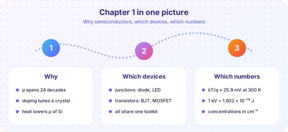
Recap table
| Lesson | Main idea | Number or formula to remember |
|---|---|---|
| Course map | Crystal, bands, doping, junction, devices | Nine chapters |
| Why semiconductors | Conductivity can be tuned | σ = q(nμn + pμp); pure Si ≈ 10⁵ Ω·cm |
| Device landscape | Two-terminal junction devices and three-terminal transistors | β = Ic/Ib; gate voltage controls MOSFET |
| Toolkit | Units and constants | 1 eV = 1.602e-19 J; kT/q ≈ 25.9 mV |
Try it
The first example is a self-test calculator: it uses the formulas of the chapter to compute a bar's resistance from its geometry and carrier data.
Press Run (or Ctrl + Enter) to see the result here.
Program input · what you'd type while the program runs
Type the answers before you press Run, one per line. Each time the program reads a line (with input()), it gets the next line from this box.
Press Run (or Ctrl + Enter) to see the console output here.
No output.
Check your understanding
Quick check · 10 questions
of 10 answered You scored / 10 · perfect!
-
1. Which statement best describes a semiconductor?
Doping, temperature, light and fields change a semiconductor's carrier density and therefore its conductivity. -
2. R = ρ L / A. If the length doubles and the area doubles, R
L/A is unchanged, so R is unchanged. -
3. Which pair of units is used for resistivity and concentration in this course?
Semiconductor engineering normally uses Ω·cm and cm⁻³. -
4. Heating a pure silicon sample
Thermal generation of carriers grows exponentially and dominates the effect of scattering. -
5. A device with two terminals whose function is to turn light into electricity is a
A solar cell is a junction with two terminals; the BJT and MOSFET have three. -
6. What does β measure for a BJT?
β = Ic/Ib is the current gain. -
7. The thermal voltage at 300 K is about
kT/q = 25.85 mV at 300 K. -
8. Which is NOT physically possible in a silicon crystal?
Silicon has only 5 × 10²² atoms per cm³, so a carrier density of 10²⁴ cm⁻³ cannot occur. -
9. LED and solar cell are related because they are
An LED turns electrical energy into light; a solar cell turns light into electrical energy. -
10. Why does 59.5 mV matter at 300 K?
V_T ln 10 ≈ 59.5 mV, so each 59.5 mV multiplies exp(V/V_T) by 10.
Summary
- Semiconductors are valuable because carrier density, and so conductivity, is tunable.
- Two families: junction devices and transistors.
- Use cm-based units and keep the key constants at hand.
- Chapter 2 opens the crystal and explains where electrons and holes come from.
Track your progress
Create a free account to tick off lessons and pick up where you left off on any device.
of Semiconductor Devices lessons completed