


















Lesson 29 of 45 · MOS Capacitors and MOSFETs
MOSFET operation: triode, saturation and the I-V equations
Derive and use the MOSFET current equations: the square-law model, triode and saturation regions, pinch-off, channel-length modulation, body effect and worked examples.
You know what the gate does to the silicon underneath it. Now add the drain. A voltage between drain and source pushes the channel electrons along, and the resulting drain current I_D depends on both V_GS and V_DS. This lesson derives the standard "square-law" model, explains why the current flattens out (saturation), and works numeric examples with the 10 nm oxide device from the last lesson.
What you will learn
- How the channel charge and drift velocity give the drain current.
- The triode and saturation equations and the condition that separates them.
- What pinch-off is and why the current stops rising with V_DS.
- Channel-length modulation, the body effect and mobility degradation as real-world corrections.
- How to extract V_T and k from measured data.
Key terms
Process transconductance parameter (k'): µ·C_ox, in A/V². For an n-channel device, k'_n = µ_n C_ox.
Device transconductance parameter (k): k' · W/L.
Pinch-off: the point where the channel charge at the drain end falls to zero as V_DS reaches V_GS − V_T.
Channel-length modulation (λ): a small increase of I_D with V_DS in saturation, because the pinched-off region grows.
Body effect: the rise of V_T when the source is at a higher potential than the body.
From channel charge to current
Suppose the gate is above threshold, so the channel contains a sheet of electrons. The mobile charge per unit area at a point x along the channel, where the channel voltage is V(x), is
Q_n(x) = −C_ox (V_GS − V_T − V(x))
The current is the product of charge per unit width, width W and drift velocity µ_n E. Because I_D is the same at every point along the channel, we can integrate from source (V = 0) to drain (V = V_DS):
I_D · L = µ_n C_ox W ∫₀^V_DS (V_GS − V_T − V) dV
which gives the triode (linear) equation
I_D = µ_n C_ox (W/L) [ (V_GS − V_T) V_DS − V_DS²/2 ], valid for V_DS < V_GS − V_T
For small V_DS the quadratic term is negligible and the transistor is a gate-controlled resistor with
R_on ≈ 1 / (µ_n C_ox (W/L) (V_GS − V_T))
Pinch-off and saturation
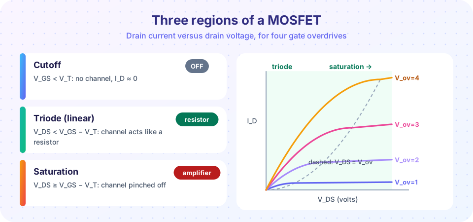
As V_DS rises, the voltage between the gate and the channel at the drain end, V_GS − V_DS, shrinks. The channel charge there, proportional to V_GS − V_T − V_DS, falls to zero when V_DS = V_GS − V_T. The channel is then pinched off at the drain. Electrons still flow: they reach the end of the thin channel and are injected into the depleted region next to the drain, where the field sweeps them to the drain contact. Increasing V_DS further moves the pinch-off point slightly toward the source but leaves the channel voltage at its pinch-off value, so the current stops changing. Putting V_DS = V_GS − V_T into the triode formula gives the saturation equation
I_D = ½ µ_n C_ox (W/L) (V_GS − V_T)², valid for V_DS ≥ V_GS − V_T
In saturation the MOSFET behaves like a voltage-controlled current source: I_D follows the square of the overdrive voltage V_ov = V_GS − V_T and ignores V_DS. This is the behavior you need for amplifiers. Compare the BJT: its collector current is exponential in the control voltage; the MOSFET's is quadratic.
Worked example
Use the device from the MOS capacitor lesson: t_ox = 10 nm (C_ox = 0.345 µF/cm²), V_T = 0.34 V, µ_n = 400 cm²/V·s (an effective channel mobility, lower than the bulk value), W/L = 10.
k'_n = 400 × 3.45e-7 = 1.38e-4 A/V² = 138 µA/V², sok_n = 138 µA/V² × 10 = 1.38 mA/V².- At V_GS = 1.5 V, V_ov = 1.16 V. In saturation
I_D = ½ × 1.38 mA/V² × 1.16² = 0.93 mA. - At V_GS = 1.5 V and V_DS = 0.1 V (triode):
I_D = 1.38e-3 × (1.16 × 0.1 − 0.005) = 0.153 mA, andR_on ≈ 1/(1.38e-3 × 1.16) = 624 Ω. - Saturation begins at
V_DS = V_ov = 1.16 V.
Real-world corrections
Channel-length modulation. Beyond pinch-off, the depleted stub grows with V_DS and the effective channel length shortens, so the current creeps upward:
I_D = ½ k (V_GS − V_T)² (1 + λ V_DS)
λ (units 1/V) is larger for short channels. The output resistance is r_o = 1/(λ I_D). With λ = 0.05 V⁻¹ and I_D = 1 mA, r_o = 20 kΩ. A longer channel reduces λ at the price of speed and area.
Body effect. If the source is not tied to the body, the source-body junction is reverse biased by V_SB, which widens the depletion region and raises V_T:
V_T = V_T0 + γ ( √(2φ_F + V_SB) − √(2φ_F) )
with body factor γ = √(2 q ε_Si N_A) / C_ox. It matters in stacked transistors such as NAND gates.
Mobility degradation and velocity saturation. A strong vertical field scatters carriers at the surface, and a strong lateral field (short channels) makes carrier velocity saturate near 10⁷ cm/s in silicon. In short devices the current grows nearly linearly with V_ov instead of quadratically, which is why modern transistors do not follow the square law exactly.
Extracting V_T. In saturation √I_D = √(k/2) (V_GS − V_T) is a straight line. Plot √I_D against V_GS, fit a line, and the x-intercept is V_T while the slope gives k. Engineers do this routinely on measured data.
Common misconceptions
"Saturation means the current is zero or the channel is closed." Saturation means the current is independent of V_DS. The channel is pinched off at one end but carries the full current.
"The MOSFET region names are the same as the BJT's." The words match, the meanings do not. A BJT in saturation is fully ON with a low V_CE; a MOSFET in saturation is the amplifier region, and the fully ON switch state is the triode region.
"The gate conducts current in a MOSFET." Only at the instant of switching (to charge the gate capacitance); in DC the gate current is essentially zero.
Try it
First, generate the output and transfer characteristics. On the right, plot √I_D against V_GS and fit the line to recover V_T and k from "measured" data (generated here with noise).
Press Run (or Ctrl + Enter) to see the result here.
Program input · what you'd type while the program runs
Type the answers before you press Run, one per line. Each time the program reads a line (with input()), it gets the next line from this box.
Now try an operating-point explorer. Choose V_GS and V_DS and the widget reports the region, I_D and the on-resistance; it uses the square-law model with λ = 0.05 V⁻¹.
Check your understanding
Quick check · 5 questions
of 5 answered You scored / 5 · perfect!
-
1. Which condition puts an n-channel MOSFET in saturation?
When V_DS reaches the overdrive voltage the channel pinches off at the drain end and the current stops depending on V_DS. -
2. k = 2 mA/V² and V_ov = 0.5 V. The saturation current (λ = 0) is
I_D = ½ k V_ov² = 0.5 × 2 mA/V² × 0.25 V² = 0.25 mA. -
3. A MOSFET in the triode region with small V_DS behaves like
For small V_DS the current is proportional to V_DS, with a resistance set by V_ov. -
4. With λ = 0.04 V⁻¹ and I_D = 0.5 mA, the output resistance r_o = 1/(λ I_D) is
1 / (0.04 × 0.5e-3) = 50 kΩ. -
5. Plotting √I_D versus V_GS in saturation gives a straight line whose x-intercept is
√I_D = √(k/2)(V_GS − V_T), which crosses zero at V_GS = V_T.
Summary
- Triode:
I_D = k[(V_GS−V_T)V_DS − V_DS²/2]forV_DS < V_GS − V_T, a gate-controlled resistor at small V_DS. - Saturation:
I_D = ½k(V_GS−V_T)²(1+λV_DS)forV_DS ≥ V_GS − V_T; the channel is pinched off. - k = µC_ox·W/L; in the worked example k = 1.38 mA/V² and a 1.5 V gate gives 0.93 mA.
- Short-channel effects (velocity saturation, mobility degradation) make real devices deviate from the square law.
- Extract V_T from the √I_D-versus-V_GS line.
Track your progress
Create a free account to tick off lessons and pick up where you left off on any device.
of Semiconductor Devices lessons completed