


















Lesson 8 of 45 · Crystals, Bands and Carriers
Energy Bands: Why Crystals Have Gaps
Understand how atomic energy levels merge into bands, what the band gap Eg means, why metals, semiconductors and insulators differ, and how Eg changes with temperature.
An isolated atom can hold its electrons only at certain energies. Bring two atoms together and each level splits into two. Bring 10²² atoms together in a cubic centimeter of crystal and each level splits into 10²² closely spaced levels that blur into a continuous band. Between some bands, no states exist at all: those ranges are gaps. The width of the gap that separates the highest filled band from the next empty one is the most important number for a semiconductor.
This lesson explains where bands come from, how to read a band diagram, and why one small number, the gap, divides all materials into three classes.
What you will learn
- How atomic levels become bands and why a gap appears.
- The meanings of Ec, Ev and Eg on a band diagram.
- How band gap separates metals, semiconductors and insulators.
- How Eg varies with temperature, and what direct and indirect gaps mean.
Key terms
- Valence band: the highest band that is full of electrons at 0 K. Its top is Ev.
- Conduction band: the next band up, empty at 0 K. Its bottom is Ec.
- Band gap Eg: Ec − Ev, the minimum energy to free an electron.
- Fermi-Dirac function f(E): the probability that a state of energy E is occupied.
From levels to bands
Two rules explain everything. First, the Pauli exclusion principle: no two electrons can occupy the same quantum state. When atoms come together, their identical energy levels cannot stay identical; each splits into a slightly different level. Second, with N atoms you get N levels per atomic level, spaced so closely that for practical purposes they form a continuous range.
In silicon the outer levels are the 3s and 3p. When the atoms are brought to the lattice spacing, these hybridize into four equivalent bonds per atom, which gives a lower band of bonding states and an upper band of antibonding states. Each atom brings four electrons, just enough to fill every bonding state. The lower band is the valence band; the upper band is the conduction band; between them lies the gap.
Reading a band diagram
A band diagram plots electron energy (up) against position (across). Two lines matter most:
- Ec: the bottom edge of the conduction band. An electron at Ec has no kinetic energy; above it, the extra energy is kinetic.
- Ev: the top edge of the valence band.
The gap Eg = Ec − Ev is a forbidden zone. An electron in the valence band needs at least Eg of energy, from heat or a photon, to jump up. After it jumps, it can move freely in the conduction band, and the empty state it left behind in the valence band is a hole (next lesson).
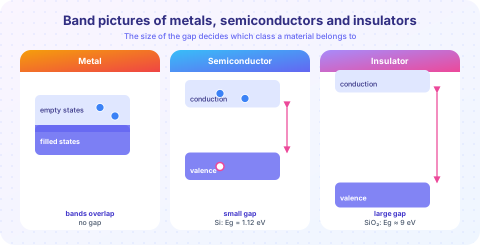
Three classes of material
| Class | Gap | Result at room temperature |
|---|---|---|
| Metal | none (bands overlap, or the top band is half full) | many free electrons always |
| Semiconductor | about 0.5 to 3 eV | few carriers, tunable |
| Insulator | more than about 4 eV | essentially none |
Typical values: Ge 0.66 eV, Si 1.12 eV, GaAs 1.42 eV, 4H-SiC 3.26 eV, GaN 3.4 eV, diamond 5.5 eV and silicon dioxide about 9 eV. The line between semiconductor and insulator is fuzzy; SiC and GaN are "wide-gap semiconductors" used in power and blue-light devices.
The thermal energy at room temperature, kT, is only 0.0259 eV. Compared with 1.12 eV, that is 43 times smaller, which is why very few electrons cross the gap in silicon.
How likely is an electron at Ec?
The Fermi-Dirac function gives the probability that a state at energy E is filled:
f(E) = 1 / (1 + exp((E − EF) / kT))
EF is the Fermi level, a reference energy at which f = ½. For a pure semiconductor, EF lies near the middle of the gap. When E − EF is more than a few kT, the function simplifies to the Boltzmann form f(E) ≈ exp(−(E − EF)/kT).
For silicon at 300 K with EF at midgap, E − EF = 0.56 eV at the bottom of the conduction band, so f(Ec) = exp(−0.56 / 0.02585) ≈ 4 × 10⁻¹⁰. A tiny probability, but there are many states, so enough carriers appear. The next two lessons make this precise.
Temperature dependence of the gap
The gap shrinks slightly as the lattice heats up and expands and vibrates. A standard empirical formula by Varshni is:
Eg(T) = Eg(0) − α T² / (T + β)
For silicon Eg(0) = 1.170 eV, α = 4.73 × 10⁻⁴ eV/K and β = 636 K, which gives 1.12 eV at 300 K and about 1.10 eV at 400 K.
Direct and indirect gaps
Electron states in a crystal are labeled by a wave vector k, a kind of momentum. If the minimum of the conduction band sits directly above the maximum of the valence band at the same k, the gap is direct: an electron can drop across and emit a photon in one step. GaAs and GaN are direct. In silicon the conduction minimum sits at a different k than the valence maximum, so the gap is indirect: the electron must also change its momentum, which needs a lattice vibration (a phonon). That makes silicon a very poor light emitter and explains why LEDs and lasers use compounds such as GaAs (chapter 7).
Try it
Press Run (or Ctrl + Enter) to see the result here.
Program input · what you'd type while the program runs
Type the answers before you press Run, one per line. Each time the program reads a line (with input()), it gets the next line from this box.
Common misconceptions
"Electrons orbit atoms in the crystal like planets." In a crystal the valence electrons are spread over the whole lattice as waves. Bands describe the allowed energies of those waves.
"The gap is a physical hole in the crystal." It is a range of energies with no allowed states, not a region of space.
Check your understanding
Quick check · 5 questions
of 5 answered You scored / 5 · perfect!
-
1. What is Eg?
The band gap is the energy difference between the bottom of the conduction band and the top of the valence band. -
2. Which principle forces atomic levels to split into bands?
Electrons cannot share a quantum state, so identical levels of many atoms spread into distinct, closely spaced levels. -
3. Why is silicon a poor light emitter?
Radiative recombination needs a momentum change in silicon, which requires a phonon and is unlikely. -
4. At 300 K and EF at midgap, the occupation probability at Ec in silicon is of order
f(Ec) ≈ exp(−0.56 / 0.0259) ≈ 4 × 10⁻¹⁰. -
5. What happens to Eg of silicon as it warms from 0 K to 300 K?
The Varshni formula gives Eg(0) = 1.17 eV and about 1.12 eV at 300 K.
Summary
- Bands arise because many atoms with identical levels must split them (Pauli principle).
- Valence band top Ev and conduction band bottom Ec bound the forbidden gap Eg.
- Metals have no gap, semiconductors about 0.5 to 3 eV, insulators more than about 4 eV.
- f(E) = 1/(1 + exp((E − EF)/kT)) gives occupation; Eg falls slowly with T (Varshni).
- Direct-gap materials (GaAs) emit light efficiently; indirect ones (Si) do not.
Track your progress
Create a free account to tick off lessons and pick up where you left off on any device.
of Semiconductor Devices lessons completed