


















Lesson 10 of 45 · Crystals, Bands and Carriers
Intrinsic Carriers: How Many Pairs in a Pure Crystal?
Calculate the carrier density of a pure semiconductor: the effective density of states Nc and Nv, the formula for ni, its temperature dependence and np = ni².
In a perfectly pure crystal, every free electron came from a broken bond, and every broken bond left a hole. So the electron and hole densities are equal: n = p = ni, the intrinsic carrier concentration. This single number, a function of band gap and temperature, sets the leakage of diodes, the limits of operating temperature, and the starting point for all doping calculations.
The calculation has three steps. Count how many conduction-band states exist near the band edge (Nc). Multiply by the occupation probability. Do the same for holes. The result is a compact formula you can use with a calculator.
What you will learn
- What the effective densities of states Nc and Nv are.
- How to compute n and p from the Fermi level.
- How ni depends on Eg and temperature, and the law n·p = ni².
- How fast ni rises with temperature, and why that limits silicon devices.
Key terms
- Intrinsic semiconductor: a pure crystal with no intentional doping.
- Nc, Nv: effective densities of states at the conduction and valence band edges (cm⁻³).
- Intrinsic carrier concentration ni: the density of electrons (equal to that of holes) in an intrinsic crystal.
- Mass-action law: n·p = ni² in thermal equilibrium.
Counting states and filling them
Near the band edge, the number of available states per unit energy grows with the square root of the energy above the edge. Integrating that density of states with the Boltzmann form of the occupation function gives:
n = Nc · exp(−(Ec − EF) / kT)
p = Nv · exp(−(EF − Ev) / kT)
The factors Nc and Nv behave like the number of states "waiting" at the band edges. They depend on effective mass and temperature:
Nc = 2 · (2π m*n k T / h²)^(3/2)
Nv = 2 · (2π m*p k T / h²)^(3/2)
Both scale as T^(3/2). Typical values at 300 K:
| Material | Eg (eV) | Nc (cm⁻³) | Nv (cm⁻³) |
|---|---|---|---|
| Si | 1.12 | 3.2 × 10¹⁹ | 1.8 × 10¹⁹ |
| Ge | 0.66 | 1.0 × 10¹⁹ | 6.0 × 10¹⁸ |
| GaAs | 1.42 | 4.7 × 10¹⁷ | 7.0 × 10¹⁸ |
(Values differ a little between references because different effective masses are used.) Notice that Nc and Nv are of order 10¹⁹ for silicon, a good fraction of the atom density: many states exist, but the occupation probability is tiny.
The intrinsic carrier concentration
In a pure crystal n = p. Multiply the two expressions: the Fermi level cancels, leaving a product that depends only on the material and temperature:
n · p = Nc Nv exp(−Eg / kT)
In a pure crystal, n = p = ni, so:
ni = √(Nc Nv) · exp(−Eg / 2kT)
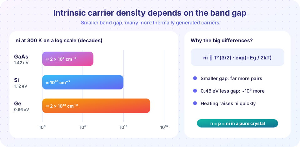
The factor 2 in the exponent appears because each pair needs one electron raised across the gap but is shared between the two carriers. For silicon at 300 K, this gives about 10¹⁰ cm⁻³ (references quote values between 6 × 10⁹ and 1.5 × 10¹⁰ depending on the constants used). For Ge, about 2 × 10¹³ cm⁻³; for GaAs, about 2 × 10⁶ cm⁻³.
Mass action and the intrinsic Fermi level
The product n·p = ni² holds not just in pure material but for any semiconductor in thermal equilibrium, even when doped. That fact, the law of mass action, is the key to doping calculations in the next chapter: if you raise n, p must fall to keep the product fixed.
For a pure crystal the Fermi level is called Ei. Setting n = p gives:
Ei = (Ec + Ev)/2 + (kT/2) · ln(Nv / Nc) = midgap + (3/4) kT ln(m*p / m*n)
So Ei is near the middle of the gap, shifted by a few meV (in silicon about 7 meV below midgap), a tiny amount compared with Eg.
Temperature dependence
ni depends on temperature through T^(3/2) and, much more strongly, through exp(−Eg / 2kT). Differentiating the logarithm at 300 K in silicon:
d ln(ni) / dT = 3/(2T) + Eg / (2kT²) ≈ 0.005 + 0.072 ≈ 0.077 per kelvin
That is about 8 percent per kelvin: ni doubles for roughly every 9 K. A silicon chip that heats from 300 K to 400 K sees ni grow by a factor of roughly 500. At high temperature the thermally generated carriers outnumber the dopants and the device loses its controlled behavior, which sets the upper operating temperature (about 150 °C for silicon). Wide-gap materials such as SiC (Eg = 3.26 eV) have vastly smaller ni at the same temperature, which is why they are used in hot environments.
Try it
The plot computes ni(T) for three materials from the formula, including the slight shrinkage of the gap with temperature.
Press Run (or Ctrl + Enter) to see the result here.
Program input · what you'd type while the program runs
Type the answers before you press Run, one per line. Each time the program reads a line (with input()), it gets the next line from this box.
Press Run (or Ctrl + Enter) to see the console output here.
No output.
Common misconceptions
"n = p = ni in every semiconductor." Only in a pure (intrinsic) one. In a doped crystal n and p differ, but their product is still ni².
"The product n·p depends on the doping." It does not. Doping shifts the balance between n and p but leaves n·p = ni² at a given temperature.
Check your understanding
Quick check · 5 questions
of 5 answered You scored / 5 · perfect!
-
1. In a pure silicon crystal at 300 K, the electron density is
Each electron came from a broken bond that also made a hole, so n = p = ni. -
2. Which formula is correct for ni?
The product n p = Nc Nv exp(−Eg/kT) equals ni², so ni has the square root and Eg/2kT. -
3. Germanium has about a thousand times more intrinsic carriers than silicon mainly because
The 0.46 eV smaller gap enters an exponential, exp(0.46 / 0.0517) ≈ 7000 before density-of-states factors. -
4. If a doped silicon sample has n = 10¹⁶ cm⁻³ at 300 K and ni = 10¹⁰ cm⁻³, then p is about
p = ni²/n = 10²⁰ / 10¹⁶ = 10⁴ cm⁻³. -
5. Roughly how much does ni of silicon change for each kelvin near 300 K?
d ln(ni)/dT ≈ 0.077 per K, so ni doubles about every 9 K.
Summary
- n = Nc exp(−(Ec − EF)/kT) and p = Nv exp(−(EF − Ev)/kT).
- ni = √(Nc Nv) exp(−Eg / 2kT); about 10¹⁰ cm⁻³ for Si, 2 × 10¹³ for Ge, 2 × 10⁶ for GaAs at 300 K.
- n·p = ni² in any equilibrium sample, doped or not.
- ni rises about 8 percent per kelvin in silicon, setting the maximum operating temperature.
Track your progress
Create a free account to tick off lessons and pick up where you left off on any device.
of Semiconductor Devices lessons completed