


















Lesson 36 of 45 · Fabrication and Scaling
Chapter overview: Fabrication and Scaling
A guide to chip manufacturing and scaling: from sand to packaged die, the key process steps, yield, Moore's law and why transistor shapes keep changing.
Everything you have learned so far assumes that someone can build a transistor with a 10 nm oxide, a base 100 nm wide or a channel a few tens of nanometers long. Making billions of these identical, on a wafer, for a few dollars per chip, is one of the great engineering achievements of our time. This chapter explains how it is done and why the transistor has kept shrinking, and what happens when shrinking runs into physics.
What you will learn in this chapter
- How silicon is purified, grown into a single crystal and cut into wafers.
- The patterning cycle (oxidation, photolithography, etching, implantation, deposition, planarization) that builds a chip layer by layer.
- Why yield depends on die area and defect density.
- Moore's law and Dennard scaling: what they said and why they slowed.
- Why transistors changed shape from planar to FinFET to gate-all-around.
Key terms
Wafer: a thin disc of single-crystal silicon, 300 mm in diameter for modern fabs, on which many chips (dies) are made at once.
Die: one chip's worth of circuitry on the wafer.
Photolithography: printing patterns with light onto a light-sensitive resist.
Yield: the fraction of dies that work.
Technology node: a generation of manufacturing process; today's names are marketing labels, not physical lengths.
The journey of a chip
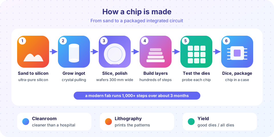
1. Silicon. Sand (SiO₂) is reduced with carbon to give metallurgical silicon, converted to a liquid compound (trichlorosilane), distilled and then decomposed back into electronic-grade polysilicon with impurities of about one atom in a billion.
2. Crystal. In the Czochralski process a small seed crystal is dipped into a crucible of molten silicon (melting point 1414 °C), rotated and slowly pulled upward. The melt freezes onto the seed in the same crystal orientation, forming an ingot of single-crystal silicon, up to 300 mm in diameter and a couple of meters long, with the desired p- or n-type doping added to the melt.
3. Wafers. The ingot is sawn into discs about 775 µm thick (for 300 mm wafers), ground, etched and polished to a surface flatter than anything else we manufacture.
4. Layers. The wafer passes through hundreds of steps in a cleanroom. The same loop is repeated for each layer: deposit a film, coat resist, expose a pattern, develop, etch or implant, strip, clean. A modern processor involves 50 to 100 mask layers and takes about three months to make.
5. Test. Probes touch each die to check it before the wafer is cut.
6. Package. Good dies are cut out, mounted on a carrier, wired or bumped to the pins, and sealed.
Sand to silicon
One perfect crystal
Layer by layer
Yield
Scaling
Lessons in this chapter
- Process steps: oxidation, lithography, implantation, diffusion, etching, deposition and planarization with numbers.
- Scaling and Moore's law: Dennard scaling, short-channel effects, high-k dielectrics and 3D transistors.
- Chapter review: recap and a ten-question quiz.
Try it
Defects kill dies. This simulation scatters random defects on a 300 mm wafer and colors every die containing a defect. It is a Monte Carlo demonstration of the Poisson yield model Y = e^(−A·D₀).
Press Run (or Ctrl + Enter) to see the result here.
Program input · what you'd type while the program runs
Type the answers before you press Run, one per line. Each time the program reads a line (with input()), it gets the next line from this box.
Now a quick economic calculator. Pick a die size and a defect density and see how many dies fit on a wafer and how many work.
Check your understanding
Quick check · 3 questions
of 3 answered You scored / 3 · perfect!
-
1. Which method grows large single-crystal silicon ingots from a melt?
A seed is dipped into molten silicon and slowly pulled and rotated, so the melt freezes in the seed's crystal orientation. -
2. Roughly how many layers of patterning does a modern processor need?
Leading-edge processes use several dozen to over a hundred masks, repeated in many process steps. -
3. What is yield?
Yield is good dies divided by total dies on the wafer.
Summary
- A chip begins as sand, becomes 9N-pure polysilicon, a Czochralski ingot and polished 300 mm wafers.
- The wafer receives dozens of patterned layers in a cleanroom; each layer repeats the same kind of loop.
- Yield falls exponentially with die area and defect density.
- Scaling made chips cheaper and faster, until physics forced new transistor shapes.
Next: Process steps
Track your progress
Create a free account to tick off lessons and pick up where you left off on any device.
of Semiconductor Devices lessons completed