


















Lesson 6 of 45 · Crystals, Bands and Carriers
Chapter 2 Overview: Crystals, Bands and Carriers
Preview chapter 2: how a silicon crystal creates energy bands, electrons and holes, and why intrinsic carrier density depends so strongly on band gap.
Every semiconductor device is built from a crystal, and every property of that crystal comes from one fact: its atoms sit on a regular lattice. The lattice turns the sharp energy levels of single atoms into broad bands, and the gap between two bands decides whether the material is a metal, a semiconductor or an insulator. This chapter builds the picture you will use for the rest of the course.
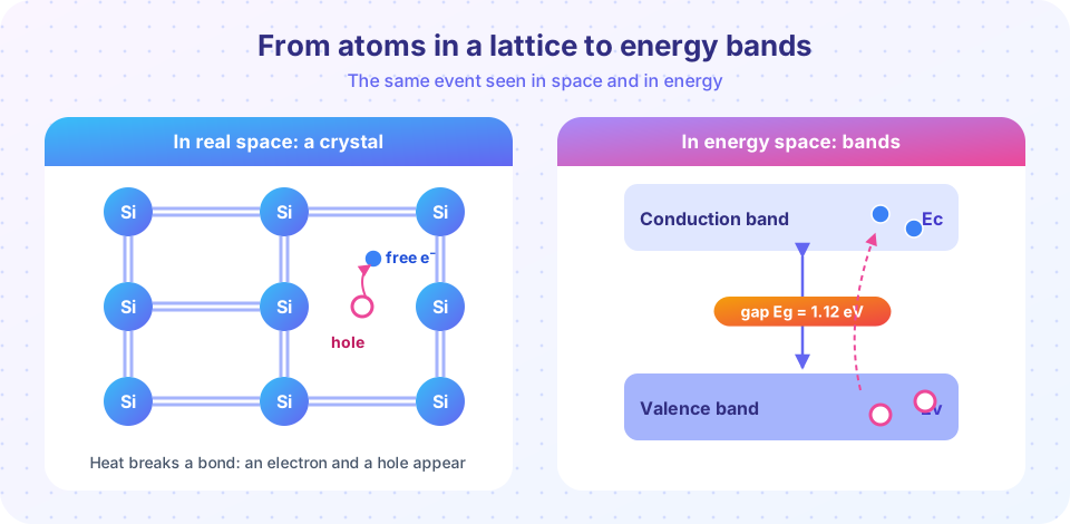
You will see the crystal twice, once in real space (atoms and bonds) and once in energy space (bands and gaps). Learning to translate between the two is the most valuable skill in this chapter.
What you will learn
- How the chapter's four lessons build on each other.
- Why band gap is the single most important number of a semiconductor.
- How to switch between a bond picture and a band picture.
- Which formulas you will meet and where to find them.
The big picture
Atoms in a lattice
Levels become bands
Carriers
Thermal generation
What each lesson covers
- Crystal structure: the diamond cubic lattice, the unit cell, covalent bonds and why silicon is a convenient material.
- Energy bands: how bands form, the band gap, and how gap size separates metals, semiconductors and insulators.
- Electrons and holes: free electrons, holes as positive carriers, and effective mass.
- Intrinsic carriers: the carrier density of a pure crystal, how it depends on temperature, and the law n·p = ni².
- Chapter review: a ten-question test and a one-page summary.
Try it
The first example is a schematic, not a simulation of real silicon. It exaggerates the number of broken bonds so you can see the trend with temperature. At 300 K the true fraction of broken bonds in silicon is around 10⁻¹³.
Press Run (or Ctrl + Enter) to see the result here.
Program input · what you'd type while the program runs
Type the answers before you press Run, one per line. Each time the program reads a line (with input()), it gets the next line from this box.
Common misconceptions
"Bands are physical layers inside the crystal." They are ranges of allowed electron energy, not regions of space. The band picture is a diagram of energy, usually drawn against position.
"A hole is a particle that exists on its own." A hole is the absence of an electron in a bond, but it behaves as a positive charge carrier, and for all circuit purposes can be treated as one.
Check your understanding
Quick check · 4 questions
of 4 answered You scored / 4 · perfect!
-
1. What does the band gap decide?
The gap between the valence and conduction bands controls how easily carriers are created. -
2. A broken bond in real space corresponds, in the band picture, to
Lifting an electron across the gap leaves an empty valence state (a hole) and a conduction electron. -
3. Which lesson introduces the law n·p = ni²?
The intrinsic carriers lesson derives how many carriers a pure crystal has and the equilibrium product. -
4. Why does the example slider show bonds breaking at higher temperature?
At higher T more electrons gain the energy needed to cross the gap, so more pairs are created.
Summary
- A crystal can be pictured as atoms and bonds, or as energy bands and a gap.
- A broken bond is a conduction electron plus a valence hole.
- Band gap sets how many carriers heat can create and which photons the material can absorb or emit.
Track your progress
Create a free account to tick off lessons and pick up where you left off on any device.
of Semiconductor Devices lessons completed