


















Lesson 39 of 45 · Fabrication and Scaling
Chapter review: Fabrication and Scaling
Review chip fabrication and scaling with a one-picture summary, a recap table of key equations, yield and cost calculators and a ten-question quiz.
You have followed silicon from sand to a packaged chip and seen why shrinking transistors both helped and hurt. This page pulls it together: one picture, a table of the numbers worth knowing, two calculators to test your intuition, and a ten-question quiz.
The chapter in one picture
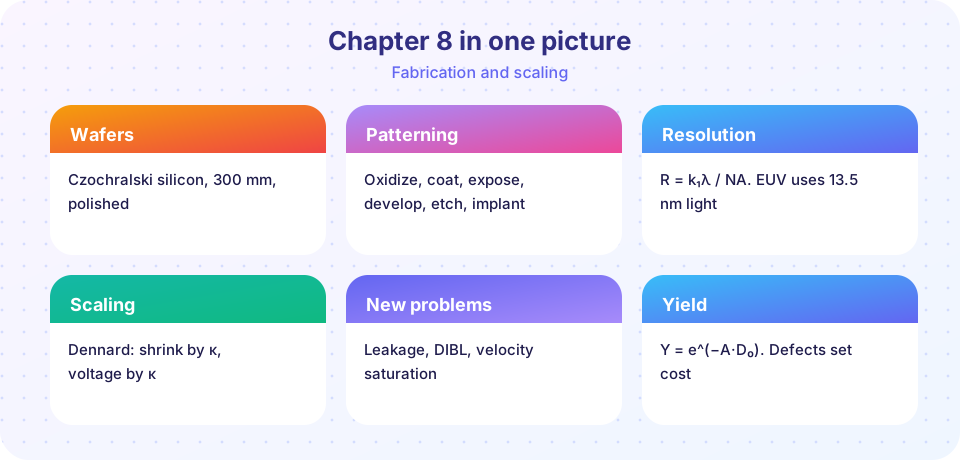
Recap table
| Topic | Key relation | Typical number |
|---|---|---|
| Crystal growth | Czochralski pulling from a 1414 °C melt | 300 mm wafers, 775 µm thick |
| Oxidation | x² + Ax = B(t + τ) |
54 nm in 1 h dry at 1000 °C, 0.43 µm wet |
| Lithography | R = k₁λ/NA |
43 nm (193i), 12 nm (EUV, k₁ = 0.3) |
| Implant | N_p ≈ 0.4Φ/ΔR_p; σ² = ΔR_p² + 2Dt |
1.1×10¹⁸ cm⁻³ for 10¹³ cm⁻² |
| Yield | Y = e^(−A·D₀) |
90.5% for 1 cm² and 0.1 cm⁻² |
| Dennard scaling | size, V × 1/κ; delay 1/κ; power density 1 | κ = 1.4 doubles density |
| Equivalent oxide | EOT = t·3.9/k |
0.59 nm for 3 nm of HfO₂ |
| Moore's law | doubling about every 2 years | 2,300 (1971) to 16 billion (2020) |
Notice how many of these formulas are exponentials: oxide and yield follow e^(...), diffusion follows exp(−E_a/kT), Moore's law is exponential in time. A small change in an input (temperature, area, defect density) can change the output by a large factor, which is why process control is so strict.
Try it
First, explore the cost side. A larger die has fewer candidates per wafer and a lower yield, so the cost per good die rises faster than the area. The wafer price here is a made-up number for illustration, so read the ratios, not the dollars.
Press Run (or Ctrl + Enter) to see the result here.
Program input · what you'd type while the program runs
Type the answers before you press Run, one per line. Each time the program reads a line (with input()), it gets the next line from this box.
Second, compare lithography options for a target pitch. For each tool the script prints the smallest half-pitch for a single exposure and the number of exposures needed for a 20 nm half-pitch pattern, using a simple model in which each extra exposure halves the pitch (a rough picture of multiple patterning).
Press Run (or Ctrl + Enter) to see the result here.
Program input · what you'd type while the program runs
Type the answers before you press Run, one per line. Each time the program reads a line (with input()), it gets the next line from this box.
Check your understanding
Quick check · 10 questions
of 10 answered You scored / 10 · perfect!
-
1. Why is the Czochralski process important?
Pulling from a melt on a seed crystal gives a defect-controlled single crystal for wafers. -
2. A 1 cm² die with D₀ = 0.2 cm⁻² has a Poisson yield of about
Y = e^(−0.2) = 0.819. -
3. Which deposition method is best for conformal atomic-scale films in deep trenches?
ALD's self-limiting reactions give uniform films of a precisely controlled thickness. -
4. With λ = 13.5 nm, NA = 0.33 and k₁ = 0.3, R is about
R = 0.3 × 13.5/0.33 = 12.3 nm. -
5. After a Dennard scaling step with κ = 2, the number of transistors per area changes by a factor of
Density scales as κ² = 4. -
6. Why did supply voltage scaling stall around 2005?
At 60 mV/decade or more, lowering V_T quickly raises off-current. -
7. EOT for a 4 nm film with k = 16 is
EOT = 4 × 3.9/16 = 0.975 nm. -
8. A gate-all-around transistor improves on a FinFET mainly by
The gate wraps each nanosheet completely, improving electrostatics. -
9. The doubling time of transistor counts in the data of this chapter is about
A log-linear fit gives close to 2 years. -
10. Annealing after implantation is needed because
Implanted dopants sit in a damaged lattice until heating restores crystal order.
Summary
- Wafers come from Czochralski ingots; chips are built by repeating deposit, pattern, etch or implant, strip.
- Resolution
R = k₁λ/NA; yieldY = e^(−A·D₀); oxide growth follows Deal-Grove kinetics. - Dennard scaling held until leakage stopped voltage scaling; new materials and 3D transistors followed.
- Next you will put your knowledge to work in practice problems and two mini-projects.
Next: Practice problem set
Track your progress
Create a free account to tick off lessons and pick up where you left off on any device.
of Semiconductor Devices lessons completed