


















Lesson 10 of 45 · Power Semiconductors
Chapter 2 Review: Power Semiconductors
Review chapter 2: the switching overlap picture, a recap table of diodes, MOSFETs, IGBTs, thyristors, SiC and GaN, a switching-energy demo and a ten-question quiz.
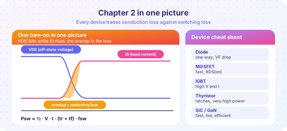
This review gathers the whole chapter into one picture and one table, then tests it. The key idea to take with you: every switch loses power in two ways. While it conducts, it wastes power through a resistance or a voltage drop. While it switches, voltage and current overlap for an instant, and the overlap becomes heat.
Chapter in one paragraph
Diodes block in one direction, with a forward drop and, for PN types, reverse recovery. MOSFETs are fast voltage-controlled switches with a resistance RDS(on), a gate charge Qg and a body diode. IGBTs trade speed for a low on-state drop at high voltage and current. Thyristors latch and handle the highest powers at line frequency. SiC and GaN, thanks to a wide bandgap, switch faster, run hotter and lose less. A device is chosen by voltage, current and frequency.
Recap table
| Device | Control | Typical strength | Typical weakness | Lesson |
|---|---|---|---|---|
| PN diode | none | high voltage, cheap | reverse recovery | Diodes |
| Schottky diode | none | low VF, no recovery | low voltage, leakage | Diodes |
| MOSFET | gate, on and off | fast, easy to drive | RDS(on) at high voltage | MOSFETs |
| IGBT | gate, on and off | low drop at high V and I | tail current, slower | IGBTs and WBG |
| Thyristor | on only | huge power, rugged | cannot turn off by gate | IGBTs and WBG |
| SiC MOSFET | gate, on and off | fast, hot, efficient | cost, gate drive care | IGBTs and WBG |
| GaN HEMT | gate, on and off | very fast, compact | low gate margin, layout | IGBTs and WBG |
The switching-loss formula, derived simply
Consider a hard-switched transistor with an inductive load. At turn-on, the current first rises to I while the voltage across the device stays at V. Then the voltage falls to zero while the current stays at I. Each phase is a triangle of power with peak V × I and duration tri or tfv, so the energy per turn-on is about
Eon ≈ ½ × V × I × (tri + tfv)
Turn-off is similar. Multiply the energy per cycle by the switching frequency to get the average power, which gives the formula used in the picture, Psw ≈ ½ V I (tr + tf) fsw. The conclusion: halve the transition time, halve the switching loss; double the frequency, double the loss.
Try it
The simulation integrates the instantaneous power of a hard-switched turn-on, using the two-phase model above, to confirm the formula numerically. It is a model with ideal piecewise-linear edges, not a measurement of a real device.
Press Run (or Ctrl + Enter) to see the result here.
Program input · what you'd type while the program runs
Type the answers before you press Run, one per line. Each time the program reads a line (with input()), it gets the next line from this box.
Check your understanding: chapter test
Quick check · 9 questions
of 9 answered You scored / 9 · perfect!
-
1. Which device is semi-controlled?
A thyristor can be turned on by the gate but only turns off when its current falls to near zero. -
2. A diode with VF = 0.8 V carries 6 A average. Approximate conduction loss?
0.8 V × 6 A = 4.8 W. -
3. Which device has no stored-charge reverse recovery?
Schottky diodes conduct with majority carriers; SiC Schottky diodes extend this to high voltage. -
4. A MOSFET has Qg = 50 nC, Vgs = 10 V and fsw = 300 kHz. Gate-drive power?
50e-9 × 10 × 300e3 = 0.15 W. -
5. Why does RDS(on) matter at the hot junction temperature?
Silicon MOSFET resistance rises with temperature; hot values should be used for loss estimates. -
6. With 300 V, 10 A and tr = tf = 25 ns at 100 kHz, what is Psw ≈ ½ V I (tr + tf) fsw?
Psw = 0.5 × 300 V × 10 A × 50 ns × 100 kHz = 1500 × 0.005 = 7.5 W. -
7. What is the tail current of an IGBT?
Stored minority carriers decay slowly after turn-off and add switching loss. -
8. Which pair describes wide-bandgap advantages?
A wider bandgap gives a higher critical field, so thinner layers, lower capacitance and faster, more efficient switching. -
9. In which application is a thyristor most appropriate?
Thyristors excel at very high power with commutation by the mains.
Summary
- Conduction loss:
I² RDS(on)for MOSFETs,VCE × Ifor IGBTs,VF × Ifor diodes. - Switching loss:
½ V I (tr + tf) fswfor hard switching; gate-drive loss:Qg Vgs fsw; diode recovery:Qrr V fsw. - Choose devices by voltage, current and frequency, with temperature margin.
- Wide-bandgap devices shift the loss trade-off toward high frequency and high temperature.
Track your progress
Create a free account to tick off lessons and pick up where you left off on any device.
of Power Electronics lessons completed