


















Lesson 28 of 45 · Control and Modulation
Voltage-mode control and small-signal models
Derive the small-signal model of a buck converter, read its LC resonance on a Bode plot, and design a type III compensator for crossover, phase margin and stability.
You have seen that a PWM modulator turns a control signal into a duty cycle. To close the loop you need to know how the output voltage responds to a small change in duty cycle, because every compensator design starts from the plant's frequency response. A switching converter is nonlinear and time-varying, which sounds hopeless, but a clever averaging step reduces it to an ordinary linear circuit around its operating point. This is the small-signal model.
In this lesson you will build that model for a buck converter, read the resonance it predicts, and design a compensator that gives a fast loop with good phase margin. The method works for every converter, only the transfer function changes.
What you will learn
- Derive the averaged equations of a buck converter and linearize them.
- Write the control-to-output transfer function and find its resonant frequency and Q.
- Define crossover frequency, phase margin and gain margin and use the usual targets.
- Place the zeros and poles of a type III compensator and check phase margin with delay.
- Explain why right-half-plane zeros limit boost and buck-boost converters.
Key terms
State-space averaging: replacing the switched circuit by its average over one period.
Control-to-output transfer function (Gvd): the small change in output voltage per small change in duty cycle.
Loop gain (T): the product of everything around the loop: compensator, modulator, plant and sensor.
Phase margin (PM): 180° + ∠T at the crossover frequency.
Right-half-plane zero: a zero that adds gain but subtracts phase, found in boost and buck-boost converters.
Averaging and linearizing the buck
Consider an ideal buck: input Vin, inductor L, capacitor C, load R. Over one period the switch is on for d·Ts. Averaging the inductor voltage and the capacitor current gives
L · diL/dt = d · Vin − vo
C · dvo/dt = iL − vo / R
These are the same equations as the circuit with an ideal voltage source d·Vin in place of the switch. At the operating point D = Vo / Vin. Now perturb: let d = D + d̂, vo = Vo + v̂o, and so on, keep only first-order terms and apply the Laplace transform. The control-to-output transfer function is
Gvd(s) = v̂o / d̂ = Vin / (1 + s·L/R + s²·L·C)
This is a second-order low-pass filter with a DC gain Vin, the resonant frequency and quality factor
f0 = 1 / (2π · √(L·C))
Q  = R · √(C / L)
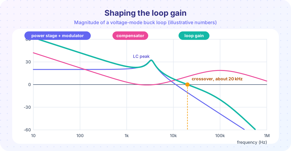
The numbers used throughout this lesson are Vin = 12 V, L = 22 µH, C = 100 µF, R = 2 Ω. They give f0 = 3.39 kHz and Q = 4.26. A Q of 4.3 means the plant has a +12.6 dB peak at f0; above it the gain falls at −40 dB per decade and the phase drops from 0° to −180° within a decade. In real converters the output capacitor's equivalent series resistance (ESR) adds a zero at fz,ESR = 1/(2π·ESR·C) that lifts the phase back; ceramic capacitors have so little ESR that the zero lies far above crossover and does not help.
The loop
The modulator contributes a gain Gm = 1 / Vramp (duty cycle per volt of control signal). With a compensator Gc(s) and a divider H (take H = 1 here), the loop gain is
T(s) = Gc(s) · Gm · Gvd(s)
Closing the loop gives vo/vref = T / (1 + T), so the loop is stable when |T| = 1 at a frequency where the phase of T is better than −180°.
- Crossover frequency
fcis where|T| = 1(0 dB). It sets the bandwidth: the loop corrects disturbances slower than aboutfc. - Phase margin
PM = 180° + ∠T(fc). Aim for45°to60°. Below 30° the transient response rings badly; at 0° the loop oscillates. - Gain margin is how much the gain could rise before the phase reaches −180°. Aim for at least 6 to 10 dB.
- A practical upper limit is
fcabout one tenth to one fifth offsw, because the modulator samples the error once per period and adds roughly a half-period delayTd ≈ Ts/2. A delay costs360° · fc · Tdof phase.
A type III compensator
Because the plant looks like 1 / (1 + s²LC) near its resonance, its phase falls to −180° and the loop would have nearly zero phase margin if you only added an integrator (which adds another −90°). The cure is a compensator that supplies a phase boost. The standard choice for voltage-mode control with a low-ESR output capacitor is type III:
Gc(s) = Kc · (1 + s/ωz1)(1 + s/ωz2) / ( s · (1 + s/ωp1)(1 + s/ωp2) )
- The integrator
1/sgives zero steady-state error and a high gain at DC. - The two zeros are placed near the plant's resonant frequency (typically at 0.5 to 1 times
f0). Each adds up to +90° of phase lead and together they cancel the double pole. - The two poles are placed well above crossover, often at the ESR zero or at
fsw/2, to attenuate switching noise and limit gain at high frequency. Kcis chosen so that|T| = 1at the wanted crossover frequency.
Design example (fsw = 200 kHz, Vramp = 1.2 V): target fc = 20 kHz, which is fsw/10.
- Design A: zeros at
0.8·f0 = 2.71 kHz, poles at 100 kHz. The plant phase at 20 kHz is −177.7°, the compensator gives−90° + 2·82.3° − 2·11.3° = +52°, soPM = 54°before delay. - Add the half-period delay
Td = 2.5 µs: it costs360 × 20,000 × 2.5e-6 = 18°, leavingPM = 36°. That is not enough. - Design B: zeros at 1.7 kHz and poles at 150 kHz recover a phase margin of about 49° including the delay.
The lesson of the example is that delay eats phase margin, and that is why crossover is held well below the switching frequency.
Boost and buck-boost converters have a right-half-plane (RHP) zero at ωz = R(1 − D)² / L (boost). Its gain rises with frequency but its phase falls, exactly the wrong direction. You must keep fc below about one third of the RHP zero frequency, which is often only a few kilohertz. This is a fundamental limit, not a design shortcut you can optimize away.
Common misconceptions
"The small-signal model is only valid for tiny changes, so it is useless." It is accurate for disturbances of a few percent, which is the regime where stability is decided. Large transients are checked by simulation.
"A higher crossover frequency always gives a better regulator." It speeds up the correction but erodes the phase margin because of delay and parasitics, and it makes the loop sensitive to noise.
"The compensator can cancel any plant pole." Cancelling is only approximate and the plant moves with load and temperature, so margins must hold across the whole operating range.
Try it
The first example computes the loop gain of the 12 V buck for the two designs, finds crossover, phase margin and gain margin numerically, and plots the Bode diagram of the delayed design B. It is a numerical frequency-response calculation of the formulas above.
Press Run (or Ctrl + Enter) to see the result here.
Program input · what you'd type while the program runs
Type the answers before you press Run, one per line. Each time the program reads a line (with input()), it gets the next line from this box.
The second example closes the loop and plots the step response of the output to a reference change, with a first-order Padé approximation for the half-period delay. It uses scipy.signal and shows how a poor phase margin rings.
Press Run (or Ctrl + Enter) to see the result here.
Program input · what you'd type while the program runs
Type the answers before you press Run, one per line. Each time the program reads a line (with input()), it gets the next line from this box.
The third example is a phase-margin calculator. Choose the crossover frequency and the compensator's zero and pole positions; the tool finds the plant's phase and the compensator's phase at crossover and reports the margin, with or without the half-period delay. It uses the same formulas as the code above.
Check your understanding
Quick check · 5 questions
of 5 answered You scored / 5 · perfect!
-
1. A buck converter has L = 10 µH and C = 47 µF. What is the LC resonant frequency?
√(10e-6 × 47e-6) = 2.17e-5, so f0 = 1 / (2π × 2.17e-5) = 7.3 kHz. -
2. What phase margin range is usually targeted?
Below about 30° the transient response rings; 45° to 60° gives a well-damped response. -
3. Why does a type III compensator have two zeros?
The two zeros near f0 supply the phase boost the LC double pole removes. -
4. A half-period delay of 2.5 µs costs how much phase at 20 kHz?
360° × 20,000 × 2.5e-6 = 18°. -
5. What is the main limitation of a boost converter's control loop?
The RHP zero adds phase lag and limits crossover to about one third of its frequency.
Summary
- Averaging and linearizing the buck gives
Gvd = Vin / (1 + sL/R + s²LC), withf0 = 1/(2π√LC)andQ = R√(C/L). - The loop gain is
Gc · Gm · Gvd; stability needs enough phase margin (45° to 60°) at the crossover frequency. - A type III compensator (integrator, two zeros near
f0, two poles high) restores the phase the LC resonance removes. - Delay of about
Ts/2costs360°·fc·Td, so crossover is held to a fraction offsw. - Boost and buck-boost have an RHP zero that limits bandwidth.
Next: Current-mode control
Track your progress
Create a free account to tick off lessons and pick up where you left off on any device.
of Power Electronics lessons completed