


















Lesson 34 of 45 · Magnetics and Thermal Design
Thermal design: losses, junction temperature and heat sinks
Estimate MOSFET conduction and switching loss, use the thermal resistance ladder to find junction temperature, choose a heat sink, and see how pulses and thermal feedback behave.
Every watt that a converter loses becomes heat, and heat must flow from the tiny silicon die to the room. Semiconductors are specified for a maximum junction temperature, typically 150 °C for silicon MOSFETs and IGBTs and up to 175 or 200 °C for silicon carbide. Operate above it and the device degrades or fails; operate hot and life shortens: a common rule of thumb is that reliability, and the life of electrolytic capacitors in particular, roughly halves for every 10 °C of extra temperature.
Thermal design is therefore a two-step calculation: first how much power is lost and where, then how large a temperature rise that power causes along the heat path. The second step is just Ohm's law with different units.
What you will learn
- Compute the conduction, switching, gate and output-capacitance losses of a MOSFET.
- Use the thermal resistance ladder to find junction, case and heat-sink temperatures.
- Choose a heat sink by calculating the maximum allowed
θSA. - Explain thermal feedback (loss that rises with temperature) and solve it iteratively.
- Use transient thermal impedance for short pulses.
Key terms
Junction temperature (Tj): the temperature of the silicon die; the number that must stay below the limit.
Thermal resistance (θ): temperature rise per watt along a path, in °C/W (equivalently K/W).
θJC, θCS, θSA: junction-to-case, case-to-sink (the interface material) and sink-to-ambient resistances.
Transient thermal impedance (Zth): the thermal resistance seen by a pulse of a given length; it is smaller than the steady-state value for short pulses.
Derating: reducing power at high ambient temperature so that Tj stays below the limit.
Where the heat comes from
For a MOSFET in a hard-switched converter the main loss terms are:
| Loss | Formula | Comment |
|---|---|---|
| Conduction | Irms² · Rds(on)(Tj) |
Rds(on) rises about 0.6 to 1 % per °C for silicon, so about 1.5 to 2 times at 125 °C |
| Switching (overlap) | ½ · Vds · Id · (tr + tf) · fsw |
voltage and current overlap during each transition |
| Output capacitance | ½ · Coss · Vds² · fsw |
energy of Coss dissipated each turn-on |
| Gate drive | Qg · Vgs · fsw |
dissipated in the gate driver and gate resistor, not mostly in the die |
| Body diode and reverse recovery | Vf · Iavg + Qrr · Vds · fsw |
during dead time and with synchronous rectifiers |
Other parts add their share: the inductor's copper and core losses, the diode's Vf·Iavg, the capacitors' Irms²·ESR, the sense resistor and the PCB traces. The sum of all of them is the efficiency loss.
Worked example (the picture). A 48 V to 12 V, 20 A buck at fsw = 200 kHz has a duty cycle D = 0.25. The high-side MOSFET carries Irms ≈ Io·√D = 10 A. With Rds(on) = 8 mΩ at 25 °C and 12 mΩ at 100 °C the conduction loss is 10² × 0.012 = 1.2 W. With tr + tf = 40 ns the overlap loss is ½ × 48 × 20 × 40e-9 × 2e5 = 3.8 W, and the Coss loss is another 0.18 W. Switching loss, not conduction loss, dominates here: a faster device or a lower frequency would help far more than a lower Rds(on).
The thermal resistance chain
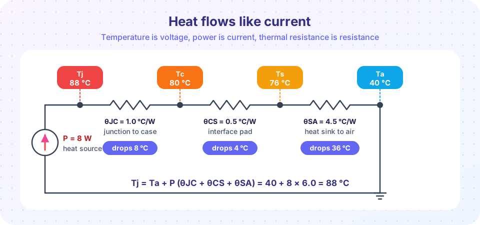
In steady state heat flows from the junction through the case, the interface and the heat sink into the ambient air. Every step has a thermal resistance, and the resistances add in series:
Tj = Ta + P · (θJC + θCS + θSA)
The figure shows an 8 W loss with θJC = 1.0 °C/W (from the datasheet), θCS = 0.5 °C/W (a thermal pad), θSA = 4.5 °C/W (a small extruded heat sink with a little airflow) and Ta = 40 °C. The temperatures are Ts = 76 °C, Tc = 80 °C and Tj = 88 °C. Notice that most of the temperature rise, 36 of 48 K, is across the heat sink: cooling is usually won or lost outside the package.
Choosing a heat sink
Rearranging, the heat sink must satisfy
θSA ≤ (Tj,max − Ta) / P − θJC − θCS
where you pick Tj,max with a margin (120 to 125 °C for a 150 °C part). For P = 5.4 W, Ta = 50 °C, Tj,max = 125 °C, θJC = 1, θCS = 0.5, the sink needs θSA ≤ 75/5.4 − 1.5 = 12.4 °C/W: a modest sink in still air. Typical orders of magnitude are: a TO-220 in free air, about 60 °C/W (junction to ambient); a small clip-on sink 15 to 25 °C/W; an extruded aluminium sink with natural convection 2 to 8 °C/W; the same with forced air 0.5 to 2 °C/W. A PCB with large copper areas can give 30 to 50 °C/W for a surface-mount power package.
Thermal feedback
Because Rds(on) increases with temperature, the loss depends on Tj, and Tj depends on the loss. Solve it by iterating: guess Tj, compute P(Tj), compute the new Tj, repeat. The iteration converges when the product of the loss's temperature sensitivity and the thermal resistance is less than one. A positive temperature coefficient of this kind is safe for a single MOSFET (hotter means more loss, but the loss grows less than the cooling), but if a heat sink is too small the iteration diverges: that is thermal runaway.
Short pulses
The steady-state θ applies only to long loads. A heat path has thermal capacitance as well, so a short pulse sees a smaller transient thermal impedance Zth(t) = Σ Ri (1 − e^(−t/τi)). A 100 W pulse lasting 1 ms heats the junction far less than 100 W applied continuously (about 40 % as much in the illustrative network of the second example below). Datasheets give Zth curves for single pulses and for various duty cycles; use them for start-up, fault and motor-stall conditions.
Heat spreads. A device on a large copper plane or a thick aluminium plate sees a lower effective θ because the heat fans out. Thermal interface material between the case and the sink should be thin and without air gaps; a dry, bare joint can add several °C/W.
Common misconceptions
"A bigger heat sink always fixes it." Past a point the interface and package resistances dominate; the junction cannot be cooler than Ta + P·(θJC + θCS).
"The case temperature is the junction temperature." The junction is hotter than the case by P·θJC. Measure the case and add that offset.
"Efficiency is a fixed number." Conduction loss rises with temperature and with load, so efficiency at a hot ambient is lower than the datasheet curve at 25 °C.
"Thermal resistance is a property of the device alone." θJA depends on the board, the airflow and the neighbouring parts.
Try it
The first example calculates the loss budget of the 48 V to 12 V buck's MOSFET, solves the thermal feedback loop and draws the graphical solution: the loss curve P(Tj) against the cooling line (Tj − Ta)/θ. Where they cross is the operating temperature. It uses an assumed Rds(on) temperature model.
Press Run (or Ctrl + Enter) to see the result here.
Program input · what you'd type while the program runs
Type the answers before you press Run, one per line. Each time the program reads a line (with input()), it gets the next line from this box.
The second example shows the transient thermal impedance of an illustrative four-stage Foster network (values chosen to sum to 1.0 °C/W, not from a datasheet) and the junction temperature rise of a 100 W pulse for several pulse lengths.
Press Run (or Ctrl + Enter) to see the result here.
Program input · what you'd type while the program runs
Type the answers before you press Run, one per line. Each time the program reads a line (with input()), it gets the next line from this box.
The third example is a heat-sink selector. Enter the loss, ambient temperature and thermal resistances, and it reports the maximum allowed θSA and what kind of cooling that suggests. The guidance ranges are rough.
Check your understanding
Quick check · 5 questions
of 5 answered You scored / 5 · perfect!
-
1. A device dissipates 6 W with θJC = 1.2, θCS = 0.4 and θSA = 3.0 °C/W at an ambient of 35 °C. What is Tj?
Tj = 35 + 6 × (1.2 + 0.4 + 3.0) = 35 + 27.6 = 62.6 °C. -
2. What is the maximum θSA for P = 10 W, Ta = 45 °C, Tj,max = 125 °C, θJC = 1.0 and θCS = 0.5 °C/W?
θSA ≤ 80/10 − 1.5 = 6.5 °C/W. -
3. A MOSFET at 400 V, 5 A with tr + tf = 30 ns and fsw = 100 kHz has an overlap loss of about
½ × 400 × 5 × 30e-9 × 1e5 = 3 W. -
4. Why can a 1 ms pulse of high power be tolerated although the same power continuously would not?
Transient thermal impedance rises with pulse length toward the steady-state value. -
5. Which statement about Rds(on) is true for silicon MOSFETs?
The positive temperature coefficient (about 0.6 to 1 % per °C) raises the loss when hot.
Summary
- Losses: conduction
Irms²·Rds(on), switching½ V I (tr+tf) fsw,Cossand gate drive, plus the magnetics and capacitors. - Steady state:
Tj = Ta + P·(θJC + θCS + θSA); the heat sink must satisfyθSA ≤ (Tj,max − Ta)/P − θJC − θCS. - Loss depends on temperature, so solve by iteration; too little cooling means thermal runaway.
- Short pulses see the transient impedance
Zth(t), much lower than the steady-state resistance. - Derate at high ambient temperature; reliability falls quickly with temperature.
Next: Chapter 7 review
Track your progress
Create a free account to tick off lessons and pick up where you left off on any device.
of Power Electronics lessons completed