


















Lesson 19 of 45 · DC-DC Converters
The Buck-Boost Converter: Up, Down and Inverted
Learn the inverting buck-boost converter: gain D/(1-D) with inverted polarity, inductor current and stresses, a runnable simulation, and Cuk, SEPIC and flyback relatives.
What if your input voltage sometimes sits above and sometimes below the output you need? A lithium-ion cell runs from 4.2 V (full) down to 3.0 V (empty), yet a microcontroller wants a steady 3.3 V. A buck cannot make more than the input, a boost cannot make less. The buck-boost converter can do both, because its gain D/(1 − D) passes through one at D = 0.5. The price is that the basic circuit inverts the polarity: the output is negative with respect to the input ground.
What you will learn
- How the inverting buck-boost works and why
Vout = −Vin D/(1 − D). - Why the energy always flows through the inductor in two separate steps.
- The currents and voltage stresses on the switch and diode.
- Related topologies: Ćuk, SEPIC, Zeta, the four-switch buck-boost and the flyback.
Key terms
- Inverting buck-boost: a converter with a switch, inductor to ground and a diode to a negative output.
- Energy transfer by the inductor: the inductor stores energy from the input, then discharges it into the output.
- Switch voltage stress: the maximum voltage the switch must block, here
Vin + |Vout|. - SEPIC and Ćuk: buck-boost relatives that keep the output polarity (SEPIC) or invert it with smooth currents (Ćuk).
- Flyback: a buck-boost with the inductor split into a transformer, adding isolation.
The two states
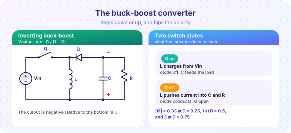
The switch Q connects the input to the inductor's top terminal; the inductor's bottom terminal goes to the common ground. The diode runs from the inductor's top terminal to the output node, with the cathode at the inductor.
- Q on (time
D T): the fullVinis acrossL, current rises with slopeVin/L. The diode is reverse-biased, since the output node is negative. The capacitor alone feeds the load. - Q off (time
(1 − D) T): the inductor current keeps flowing in the same direction, which pulls the inductor's top terminal below ground until the diode conducts. The inductor now delivers its current into the output capacitor and load, with voltage−|Vout|across it, so the current falls.
Volt-second balance gives Vin D T = |Vout| (1 − D) T, so
Vout = −Vin × D / (1 − D)
| D | Gain magnitude | Behavior |
|---|---|---|
| 0.25 | 0.33 | steps down |
| 0.5 | 1 | same magnitude as the input |
| 0.75 | 3 | steps up |
Currents. In steady state, the average diode current equals the output current, and the diode carries the inductor current only during the off time: Iout = IL (1 − D), so IL = Iout / (1 − D). Since Pin = Pout, the input current is Iin = IL D = Iout D / (1 − D). The ripple is the same as in the boost: ΔIL = Vin D / (L fsw), and the output ripple is ΔVout ≈ Iout D / (fsw C).
Stress. Both the switch and the diode must block Vin + |Vout|, which is more than in the buck or the boost. A 12 V to −12 V converter needs devices rated well above 24 V.
Design example
Make −12 V at 1 A from Vin = 12 V at fsw = 100 kHz.
D = |Vout| / (Vin + |Vout|) = 12 / 24 = 0.5.IL = Iout / (1 − D) = 2 A. The average input current isIin = IL × D = 1 A, drawn as pulses of about 2 A while the switch is on.- Ripple of 30%:
ΔIL = 0.6 A,L = Vin D / (fsw ΔIL) = 12 × 0.5 / (100 kHz × 0.6 A) = 100 µH. - Peak current:
2 + 0.3 = 2.3 A: choose an inductor for 3 A saturation. - Output ripple
50 mV:C = Iout D / (fsw ΔV) = 1 × 0.5 / (100 kHz × 0.05) = 100 µF. - Device voltage:
24 Vplus a margin, so 40 V parts.
The relatives
- Four-switch (non-inverting) buck-boost: a buck stage and a boost stage sharing one inductor. The output keeps the input's polarity. It buck-operates when
Vin > Voutand boost-operates whenVin < Vout. Common in battery-powered products and USB-C power delivery. - SEPIC (single-ended primary-inductor converter): two inductors and a coupling capacitor. Non-inverting, can step up or down, and the input current is smooth.
- Ćuk converter: also uses two inductors and a coupling capacitor, but inverts. Both input and output currents are smooth, so it is quiet, at the cost of more parts.
- Zeta converter: non-inverting, with smooth output current.
- Flyback: replace the inductor by a transformer with two windings. Energy is stored in the core during the on time and released through the secondary during the off time. It gives galvanic isolation, and its gain is scaled by the turns ratio:
Vout = Vin × (N2/N1) × D/(1 − D). The flyback is the most common isolated converter below about 100 W, found in phone chargers.
Common misconceptions
- "The buck-boost output is simply a flipped boost." The topologies differ: in the buck-boost, the inductor never connects the input and the output at the same time, so the input current is pulsed (unlike the boost) and the switch sees
Vin + |Vout|. - "A negative output is a defect." It is often exactly what you need, for example a −5 V or −12 V rail for analog circuits. Where it is not wanted, use a non-inverting relative.
Try it
The simulation below integrates the inverting buck-boost with an ideal switch and diode (the output voltage is plotted as a magnitude), and compares the numbers with the formulas from this lesson. This is a model of the ideal circuit without losses.
Press Run (or Ctrl + Enter) to see the result here.
Program input · what you'd type while the program runs
Type the answers before you press Run, one per line. Each time the program reads a line (with input()), it gets the next line from this box.
The second tool helps you choose a topology from an input range and a target output. It is a rule-based helper to practice the ideas, not a design tool.
Press Run (or Ctrl + Enter) to see the console output here.
No output.
Check your understanding
Quick check · 5 questions
of 5 answered You scored / 5 · perfect!
-
1. An inverting buck-boost with Vin = 10 V runs at D = 0.6. What is Vout?
|Vout| = Vin D/(1 − D) = 10 × 0.6/0.4 = 15 V, inverted. -
2. What voltage must the switch of an inverting buck-boost block?
When the switch is off, the input voltage adds to the negative output. -
3. For Vout = −12 V from Vin = 12 V at 1 A out, what is the average inductor current?
IL = Iout / (1 − D) = 1 / 0.5 = 2 A. -
4. Which converter keeps the output polarity and can step up or down?
A SEPIC (or four-switch buck-boost) is non-inverting and can step up or down. -
5. What does a flyback converter add to the buck-boost idea?
The flyback replaces the inductor with a coupled-inductor transformer.
Summary
- Buck-boost gain is
−D/(1 − D): below one forD < 0.5, above one forD > 0.5, with inverted polarity. - Energy goes input to inductor, then inductor to output; input and output are never connected directly.
IL = Iout/(1 − D); the switch and diode blockVin + |Vout|.- SEPIC, Ćuk, Zeta and the four-switch buck-boost give variations; the flyback adds isolation.
Track your progress
Create a free account to tick off lessons and pick up where you left off on any device.
of Power Electronics lessons completed