


















Lesson 39 of 45 · Applications: Solar, EVs and Power Supplies
Switching power supplies and PFC
Follow an offline switching supply from the wall to a USB-C port: rectifier, power factor correction, flyback design equations, power factor and THD, standby and safety.
The charger for a laptop or phone is a miniature power-electronics system: it takes 85 to 265 V AC from the wall, isolates it, steps it down to 5 to 20 V DC, regulates it to a percent, passes safety tests and costs a few dollars. The older heavy "wall wart" used a 50 Hz transformer and a linear regulator; the modern one is a switched-mode power supply (SMPS) with a ferrite transformer operating at tens or hundreds of kilohertz, small enough to disappear in a plug.
Two ideas matter most: isolation (a transformer within a flyback or LLC converter) and power factor correction (a boost stage that tells the mains the supply is a resistor). In this lesson you will see why PFC is needed, how a flyback is designed from a specification, and why modern chargers shrank so dramatically.
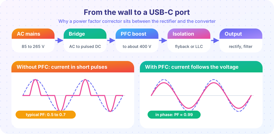
What you will learn
- Describe the stages of an offline supply and what each does.
- Define power factor, distortion factor and THD and calculate PF from them.
- Explain why a capacitor-input rectifier has a poor power factor and how a boost PFC fixes it.
- Design a flyback converter from a specification: turns ratio, duty cycle, primary inductance and stresses.
- Describe standby power and safety requirements.
Key terms
Power factor (PF): real power divided by apparent power, PF = P / (Vrms · Irms).
Distortion factor: the ratio I1,rms / Irms of the fundamental to the total rms current.
THD (total harmonic distortion): for the current, THDi = √(Irms² − I1,rms²) / I1,rms.
Flyback converter: an isolated converter in which a coupled inductor stores energy while the switch is on and delivers it to the output while it is off.
Reflected voltage (Vor): the output voltage multiplied by the turns ratio, seen by the primary switch during the off time.
From the wall to the output
- Input protection and EMI filter. A fuse, a surge and inrush limiter (an NTC thermistor or a relay-bypassed resistor) and a common-mode choke with X and Y capacitors keep switching noise out of the mains.
- Bridge rectifier. Four diodes turn the AC into a pulsating DC of up to
√2 × 265 = 375 Vpeak. - PFC stage (for supplies above roughly 75 to 100 W): a boost converter that shapes the input current and regulates a bulk voltage of about 400 V.
- Isolated DC-DC stage. A flyback (up to about 100 W), a forward converter, a half-bridge, or an LLC resonant converter (hundreds of watts and up). The transformer provides the galvanic isolation required for touch-safe outputs.
- Secondary rectification and filter. A Schottky diode or, at high efficiency, a synchronous rectifier MOSFET, then an output capacitor.
- Feedback across the isolation barrier: an optocoupler with a shunt regulator, or regulation sensed from the primary-side auxiliary winding.
Modern chargers use wide-bandgap devices. A GaN transistor switches fast with small capacitances, allowing 100 to 300 kHz or more with high efficiency, so the transformer and capacitors shrink. A 65 W USB-C charger today is a fraction of the volume of its predecessor from a decade ago.
Power factor
A resistive load draws a current proportional to the voltage and has PF = 1. A simple rectifier with a bulk capacitor draws current only when the mains voltage exceeds the capacitor voltage, in narrow pulses near the peaks (see the left plot of the figure). The pulses have the same average power as a sine but a much larger rms value, so the same power needs a larger current: heavier wiring, higher losses in the grid, and harmonic currents (3rd, 5th, 7th, …) that distort the network voltage.
Define the displacement factor cos φ (the phase angle between the fundamental of the current and the voltage) and the distortion factor I1,rms / Irms. Then
PF = P / (Vrms · Irms) = (I1,rms / Irms) · cos φ = cos φ / √(1 + THDi²)
A capacitor-input rectifier has almost no phase shift (cos φ ≈ 1) but THDi of 100 % or more, so PF ≈ 0.5 to 0.7. A well-designed PFC stage gets THDi below 10 % and PF > 0.99. Regulations such as IEC 61000-3-2 set limits on the harmonic currents of equipment above 75 W or so, and most larger supplies therefore carry a PFC stage.
The boost PFC
The PFC stage is the boost converter of Chapter 4 with a clever controller. The rectified mains voltage |vin(t)| is the boost input; the output is a bulk capacitor at about 400 V, higher than the 325 V peak of 230 V mains, as a boost requires. An inner current loop forces the inductor current to follow a reference iref = k · |vin| that is proportional to the rectified voltage, and a slow outer voltage loop sets k to regulate the bulk voltage. The converter therefore looks like a resistor, Reff = Vin² / P, to the grid: that is how power factor is corrected. Because the output has to be held steady, a bulk capacitor buffers the 100 or 120 Hz power pulsation, as in solar inverters. At low power a boundary-conduction mode controller switches when the inductor current reaches zero; at high power continuous-conduction mode with average-current control is used, and the totem-pole bridgeless topology with GaN or SiC removes the diode bridge and reaches 99 % efficiency.
Designing a flyback
In a flyback the transformer is really a coupled inductor with an air gap. When the primary switch is on, the primary current ramps up and energy is stored; when it turns off, the stored energy flows out through the secondary diode. In continuous conduction mode:
Vo = Vin · (Ns / Np) · D / (1 − D)           (n = Np / Ns)
Vor = n · (Vo + Vf)                           (reflected voltage during the off time)
Vds,max ≈ Vin,max + Vor + Vspike              (voltage across the primary switch)
Example: a 65 W USB-C supply, 20 V at 3.25 A, with the rectified input between 100 V (at 90 V AC, low line, after ripple) and 375 V (at 265 V AC).
- Choose
n = 5. With a 0.7 V diode drop,Vor = 5 × 20.7 = 103.5 V. - At low line the duty cycle is
D = Vor / (Vor + Vin,min) = 103.5 / 203.5 = 0.51. - Input power at 90 % efficiency is
65/0.9 = 72 W. At the boundary of conduction,Pin = ½·Vin·Ip,pk·D, soIp,pk = 2 × 72 / (100 × 0.51) = 2.8 A. - The primary inductance for a 100 kHz switching frequency at low line is
Lp = Vin·D / (Ip,pk·fsw) = 100 × 0.51 / (2.8 × 1e5) = 180 µH. - The switch must withstand
375 + 103.5 + ~80 Vof leakage spike = about 560 V, so a 650 V MOSFET is just adequate and a clamp or snubber is essential. - The secondary peak current is
n · Ip,pk = 14 Aand the secondary diode or synchronous rectifier seesVo + Vin,max/n = 20 + 75 = 95 V: a 100 V device (or 120 V with margin).
The transformer is then designed as in the previous chapter: the primary needs a gapped core that stores ½·Lp·Ip,pk² = 0.7 mJ, with turns chosen so that Bpk stays below the limit.
Standby, efficiency and safety
- No-load power. An adapter plugged in all day should draw well under a watt, preferably under 0.1 W. Controllers enter burst mode at light load, switching in bursts to reduce the losses per cycle. Regulations in most regions limit no-load power and set minimum average efficiency.
- EMC. The fast edges create conducted and radiated noise, so layouts, filters, Y capacitors and shielding are part of the design, not an afterthought.
- Safety. Reinforced isolation between mains and the output, creepage and clearance distances, a fuse, over-temperature, over-voltage and short-circuit protection are required by safety standards and tested for.
- Efficiency. Modern chargers reach 92 to 95 % at full load. Every percent matters, because the 5 % that is lost in a 65 W charger is 3 W of heat in a sealed plastic case.
Common misconceptions
"Power factor correction saves energy at the meter." For a home it does not change the energy used by the load; it reduces the current drawn from the grid and the harmonic distortion. The saving is in the network.
"Flyback means the transformer stores energy." In a flyback it does (it is a coupled inductor); in a forward or LLC converter the transformer transfers energy and stores almost none.
"A bigger bulk capacitor improves power factor." It does the opposite: it makes the current pulses narrower and taller.
Try it
The first example simulates a bridge rectifier with a bulk capacitor on 230 V, 50 Hz mains and computes the power factor and the current THD for several capacitor sizes, then compares with an ideal PFC that draws a sinusoidal current. It is a time-domain simulation with an ideal bridge and a small source resistance.
Press Run (or Ctrl + Enter) to see the result here.
Program input · what you'd type while the program runs
Type the answers before you press Run, one per line. Each time the program reads a line (with input()), it gets the next line from this box.
The second example is a flyback design calculator. Enter the specification; it computes the duty cycle, peak currents, primary inductance and voltage stresses at boundary conduction and plots one switching period of the primary and secondary currents. It uses the textbook equations above and is a first estimate, not a finished design.
Press Run (or Ctrl + Enter) to see the result here.
Program input · what you'd type while the program runs
Type the answers before you press Run, one per line. Each time the program reads a line (with input()), it gets the next line from this box.
The third example turns the power-factor formula into a calculator. Choose the current THD and the displacement angle, and read the power factor.
Check your understanding
Quick check · 5 questions
of 5 answered You scored / 5 · perfect!
-
1. A rectifier has THDi = 100 % and cos φ = 1. What is the power factor?
PF = 1 / √(1 + 1²) = 0.707. -
2. A flyback has Vo = 12 V, Vf = 0.5 V and n = Np/Ns = 8. What is the reflected voltage?
Vor = n (Vo + Vf) = 8 × 12.5 = 100 V. -
3. Why does the PFC boost stage need an output higher than the mains peak?
The 400 V bulk voltage exceeds the 325 V peak of 230 V mains. -
4. What is the main benefit of a synchronous rectifier on the secondary?
A MOSFET with a low Rds(on) drops less voltage than a Schottky diode. -
5. Why do chargers burst-mode at light load?
Switching in occasional bursts reduces the per-cycle losses when little power is needed.
Summary
- An offline supply chains an EMI filter, rectifier, PFC boost, an isolated stage (flyback, LLC) and a secondary rectifier with isolated feedback.
PF = cos φ / √(1 + THDi²); a capacitor-input rectifier hasPFabout 0.5 to 0.7, a boost PFC above 0.99.- Flyback:
Vor = n(Vo + Vf),D = Vor/(Vor + Vin),Vds,max ≈ Vin,max + Vor + spike,Lp = Vin·D/(Ip·fsw)at boundary conduction. - GaN and SiC, higher switching frequencies and synchronous rectification make modern chargers small and efficient; burst mode keeps standby power low.
Next: Chapter 8 review
Track your progress
Create a free account to tick off lessons and pick up where you left off on any device.
of Power Electronics lessons completed