


















Lesson 17 of 45 · DC-DC Converters
The Buck Converter: Stepping Voltage Down
Learn the buck converter from first principles: volt-second balance, inductor ripple, capacitor ripple, sizing L and C, CCM versus DCM, with a runnable simulation.
The buck converter is the most widely used switching converter in the world. Every time you see a small board that makes 5 V, 3.3 V or 1 V from a higher voltage, it is very likely a buck. It takes a higher DC input, chops it with one switch, and averages the pulses with an inductor and capacitor to deliver a lower, regulated output at high efficiency.
What you will learn
- How the buck works in the two switch states.
- Why
Vout = D × Vinand how to compute inductor and capacitor ripple. - How to size
LandCfor a given spec. - What changes in discontinuous conduction mode (DCM).
Key terms
- Freewheeling diode: carries the inductor current while the switch is off.
- Inductor ripple current (ΔIL): peak-to-peak variation of inductor current.
- Critical inductance: the inductance at the boundary between CCM and DCM.
- Synchronous buck: a buck in which the diode is replaced by a second MOSFET to cut loss.
- Saturation current: the inductor current at which its inductance collapses.
The circuit and its two states
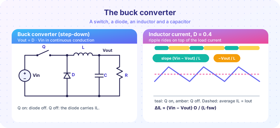
The switch Q connects the input to the inductor L. The diode D sits between the switch node and ground. The capacitor C and the load R sit at the output.
- Q on (time
D T): the input pushes current intoL. The diode is reverse-biased. The inductor voltage isVin − Vout, so the current rises with slope(Vin − Vout)/L. - Q off (time
(1 − D) T): the inductor insists on continuing its current, so the switch node falls until the diode turns on. The inductor voltage is−Vout(ignoring the diode drop), so the current falls with slope−Vout/L.
Voltage gain. Volt-second balance on L: (Vin − Vout) D T = Vout (1 − D) T. Solving gives Vout = D × Vin.
Inductor ripple. During the on time, the current rises by
ΔIL = (Vin − Vout) × D T / L = (Vin − Vout) × D / (L × fsw)
The average inductor current equals the load current Iout. The peak is Iout + ΔIL/2 and the minimum is Iout − ΔIL/2.
Capacitor ripple. The capacitor absorbs the ripple part of the inductor current (it sees the load as DC). The charge added in each half-triangle gives
ΔVout ≈ ΔIL / (8 × fsw × C) (ideal capacitor, no ESR)
and a real capacitor adds ΔIL × ESR.
Design example
Design a converter for Vin = 12 V, Vout = 5 V, Iout = 2 A, fsw = 500 kHz.
- Duty cycle:
D = 5/12 = 0.417. - Choose ripple of about 30% of load current:
ΔIL = 0.6 A. - Inductance:
L = (Vin − Vout) D / (fsw ΔIL) = 7 × 0.417 / (500 kHz × 0.6 A) = 9.7 µH. Pick10 µH:ΔIL = 0.583 A. - Peak inductor current:
2 + 0.29 = 2.29 A. Choose an inductor with a saturation current of at least 3 A, and a rating for the rms current of 2 A. - Output ripple target
20 mV:C = ΔIL / (8 fsw ΔV) = 0.583 / (8 × 500 kHz × 0.02 V) = 7.3 µF. In practice, ESR dominates, so use a ceramic capacitor of 22 µF, with very low ESR. - Continuous mode down to
Iout = ΔIL/2 = 0.29 A. Below that the converter enters DCM.
Notice the trade-off: doubling fsw halves L and C for the same ripple. Larger L reduces ripple but slows the converter's response to load steps.
Critical inductance and discontinuous mode
The boundary of CCM is where the inductor current just touches zero at the end of the off time: Iout = ΔIL/2. The critical inductance for a given load resistance R is
Lcrit = (1 − D) R / (2 fsw)
If L > Lcrit the converter is in CCM. Otherwise it is in DCM, where the inductor current sits at zero for part of the off time. The gain in DCM depends on the load: with K = 2 L / (R T),
Vout / Vin = 2 / (1 + √(1 + 4K / D²))
which is higher than D and increases as the load gets lighter. A buck converter whose controller assumes Vout = D Vin would let the output rise at light load if it did not use feedback; this is one reason regulation needs a feedback loop (chapter 6).
Synchronous buck
At low output voltage and high current, the freewheeling diode loses VF × Iout × (1 − D): for 1.2 V out from 12 V, 0.5 V × 20 A × 0.9 = 9 W, which is a lot. Replacing it with a second MOSFET (the "low-side" switch), turned on while the high-side is off, drops the loss to I² RDS(on). The drawback is dead time: both MOSFETs must never conduct together, so a short gap with both off lets the body diode conduct briefly.
Common misconceptions
- "Vout = D Vin always." It is true in CCM. In DCM at light load, the output is higher than
D Vinunless feedback reducesD. - "The input current is smooth." The input current is a pulsed current (the switch interrupts it), so a buck needs a good input capacitor, often a larger one than the output capacitor.
Try it
The simulation below integrates the equations of the buck converter's inductor and capacitor with an ideal switch and diode, the same model used in the volt-second derivation. The first run uses a heavy load, giving CCM; the second uses a light load, giving DCM where the output rises above D × Vin. This is a numerical model of an ideal circuit (no switch resistance or diode drop).
Press Run (or Ctrl + Enter) to see the result here.
Program input · what you'd type while the program runs
Type the answers before you press Run, one per line. Each time the program reads a line (with input()), it gets the next line from this box.
The design equations are easy to turn into a calculator. Change the numbers to see how frequency, inductance and capacitance shape the ripple.
Check your understanding
Quick check · 5 questions
of 5 answered You scored / 5 · perfect!
-
1. A buck converter runs from 24 V with D = 0.25 in CCM. What is Vout?
Vout = D × Vin = 0.25 × 24 = 6 V. -
2. Vin = 12 V, Vout = 3 V, L = 10 µH, fsw = 400 kHz. What is the inductor ripple ΔIL?
D = 0.25, ΔIL = (12 − 3) × 0.25 / (10e-6 × 400e3) = 2.25 / 4 = 0.5625 A. -
3. What happens to the inductor ripple if you double the switching frequency?
ΔIL is inversely proportional to L × fsw. -
4. At the CCM/DCM boundary, the load current equals:
The inductor valley current is Iout − ΔIL/2. When that reaches zero, Iout = ΔIL/2. -
5. Why use a synchronous buck at low output voltage?
The diode drop is a larger fraction of a low output voltage, so replacing it with a low-resistance MOSFET raises efficiency.
Summary
- Buck gain is
D; it steps down only. ΔIL = (Vin − Vout) D / (L fsw),ΔVout ≈ ΔIL / (8 fsw C)plus ESR.- The CCM boundary is
Iout = ΔIL/2; below it, DCM raises the gain aboveD. - Synchronous rectification replaces the diode by a MOSFET to cut loss.
- Pick
Lfrom the ripple budget and the saturation current from the peak current.
Next: The Boost Converter
Track your progress
Create a free account to tick off lessons and pick up where you left off on any device.
of Power Electronics lessons completed